
Dragonfly® G3 System
Highly configurable, automated, high speed 2D inspection and 3D metrology for inline process control in advanced packaging, specialty and front-end OQA.

Specialty devices are the unsung heroes of modern life. For many in the semiconductor industry today, the spotlight is on the SiC and GaN power devices used in automotive, green energy, fast-charge consumer electronics (CE), and high-performance computing (HPC) applications.

May 5 — May 7, 2026
Onto Innovation is a proud exhibitor at SEMICON Southeast Asia.
The Dragonfly G5 system is engineered for inline process control of leading-edge advanced packaging technologies. As the latest generation pattern inspection system in the Dragonfly series, it delivers unparalleled accuracy in detecting submicron defects and performing high-resolution 3D measurements.
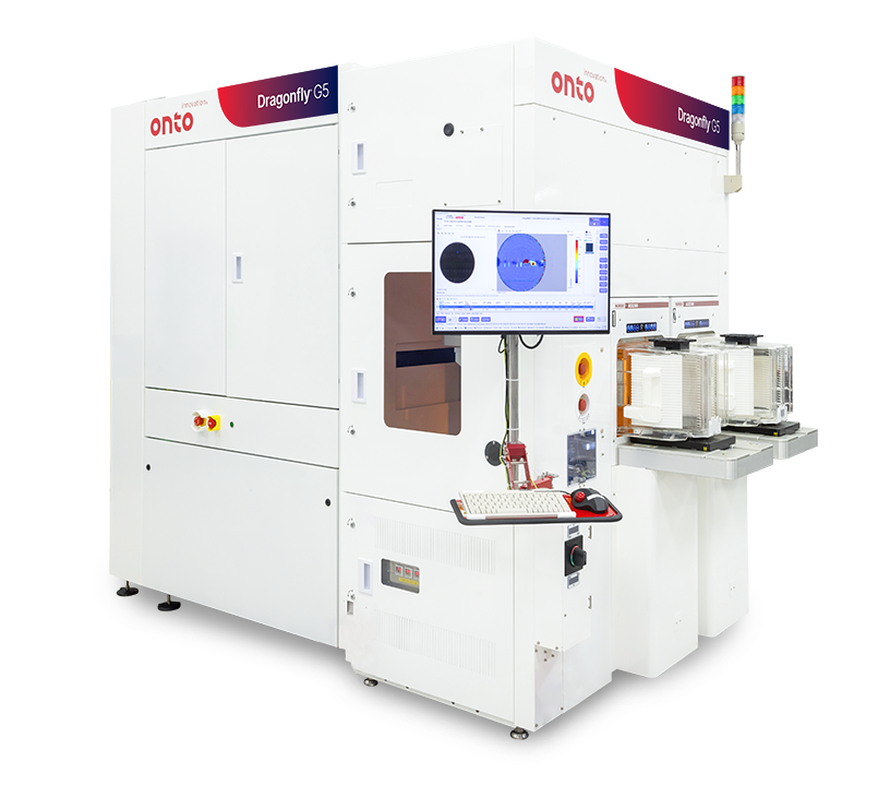
Designed to meet the demands of advanced semiconductor technologies, the Dragonfly G5 system is purpose-built to deliver high-performance, reliable inspection and metrology across complex heterogeneous integration processes. Leveraging next generation high speed line scan 2D imaging and custom-engineered objectives, the system achieves over 3X throughput improvement compared to its predecessor, with submicron sensitivity down to 150nm.
Continuing the legacy of innovation, the Dragonfly G5 system introduces a multi-angle illumination channel that significantly improves signal-to-noise ratio for faint defect detection. Combined with powerful AI-driven algorithms, it enhances both the detectability and classification of critical, yield-impacting defects–empowering fabs to maintain quality and accelerate time-to-yield.
The Dragonfly G5 system expands process control flexibility for wafer-to-wafer and die-to-wafer bonding by integrating high-speed IR imaging to detect sub-surface defects. It incorporates the latest generation of 3Di™ technology, extending bump height metrology capabilities to support next-generation microbumps essential for 3D integration. This enables additional inspection and metrology touchpoints across increasingly complex packaging architectures.


Hybrid bonding enables ultra-dense 3D memory interconnects with up to 1,000x more connections than microbumps. Achieving high yield requires stringent process control, including monitoring topography and detecting particles, cracks and voids. Measuring dishing in copper pads provides valuable insight into surface conditions. Together, these process control insights contribute to improved device reliability and performance.

As demand grows for high-performance computing (HPC) and AI-driven applications, manufacturers are turning to hybrid bonding to enable the ultra-dense 3D integration required for next-generation chip architectures. This advanced packaging technology presents significant process challenges. Surface preparation must be precisely controlled to eliminate particles, excess recess, and copper pad dishing, all of which can compromise bond quality. During pre-annealing, particle-induced gaps and wide bonding gaps can prevent proper wafer contact. Post-annealing, the formation of dielectric and metal voids introduces further risks to electrical performance and long-term reliability.

The Iris S system is a versatile platform solution for the advanced packaging and specialty market, supporting 150mm, 200mm and 300mm wafers. It provides thin and thick film, OCD and wafer bow and film stress measurements.

The IMPULSE V system helps to advance CMP processing with enhanced wavefront technology and AI-driven analytics, delivering over 2X precision improvement and faster solutions, crucial for next-gen semiconductor manufacturing demands.

The Dragonfly G5 system is engineered for inline process control of leading-edge advanced packaging technologies. As the latest generation pattern inspection system in the Dragonfly series, it delivers unparalleled accuracy in detecting submicron defects and performing high-resolution 3D measurements.

The Aspect System is a revolutionary in-line, non-destructive infrared optical critical dimension (IRCD) system measuring Z-dimension profiling of high aspect ratio structures to enable critical process control. It meets the needs of leading-edge customers with its high speed and process coverage.

As your partner for innovative solutions, we’re always here for you.
Discover how our cutting-edge semiconductor solutions are engineered to meet your most complex challenges: delivering performance, reliability and innovation where it matters most.
"*" indicates required fields
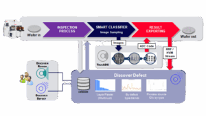
The native integration of the Discover software platform boosts tool throughput and enhances inspection quality by capturing more defects of interest. It provides a complete reduced review solution utilizing advanced machine learning (ML) and artificial intelligence (AI) technologies, customized to meet unique customer needs.
Optimized Image Capture for Inspection Tools
Discover software enhances inspection quality and tool throughput by optimizing the image capture sample plan.
AI-Powered Automatic Defect Classification (TrueADC Software)
Integrated AI-based classification improves device quality and yield, driving fab efficiency and productivity.
Streamlined Review Software
Reduced review best practices improve operator productivity, enhance engineering review quality, and shorten review time.
Advanced Defect Analytics
Comprehensive inline wafer/panel monitoring enables automatic alarm notifications, detailed reports and Out-of-Control Action Plans (OCAPs).
Defect Source Analysis
Enables actionable process feedback to improve manufacturing outcomes.
Automated Business Analysis with Report Server
Boosts engineering productivity by up to 25% and supports multiple production report formats.
Machine Learning-Based Pattern Detection
The Discover Patterns software module proactively identifies wafer-level systematic yield-limiting issues and classifies them for analytics, enabling both process feedback and feedforward.
Centralized Defect & Metrology Management
Built on a scalable Big Data and high-availability architecture, this solution supports advanced applications such as high volume manufacturing (HVM) bump metrology, capable of handling wafers with over 100 million bumps.

As your partner for innovative solutions, we’re always here for you.
Discover how our cutting-edge semiconductor solutions are engineered to meet your most complex challenges: delivering performance, reliability and innovation where it matters most.
"*" indicates required fields
The PrimaScan wafer defect inspection system delivers a flexible, high sensitivity solution at the lowest cost of ownership per pass.
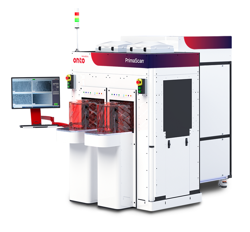
The PrimaScan system utilizes laser scatterometry and imaging techniques leveraging proprietary optics and sensing technologies for reliable inspection of nanometer sized defects on a variety of opaque and transparent/semi-transparent substrates suitable for either R&D or high-volume manufacturing environments. With multiple detection channels, the system can detect, measure, characterize and image surface particles, scratches, pits, bumps, surface contamination, film or bulk wafer stress, voids/inclusions, including chips and cracks at the wafer edge.
The PrimaScan system addresses challenges in both incoming wafer quality control and in inline process monitoring. Capable of handling multiple substrate materials, it uniquely addresses inline process defect and contamination monitoring in wafer-based production environments.
Designed with versatility in mind the PrimaScan system can handle a variety of wafer sizes and substrate types


As your partner for innovative solutions, we’re always here for you.
Discover how our cutting-edge semiconductor solutions are engineered to meet your most complex challenges: delivering performance, reliability and innovation where it matters most.
"*" indicates required fields
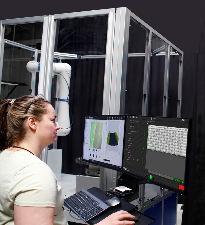
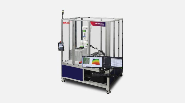
The 4Di InSpec AMS qualifies features and defects on complex geometries and in difficult-to-reach locations – hundreds of times faster than manual inspection.
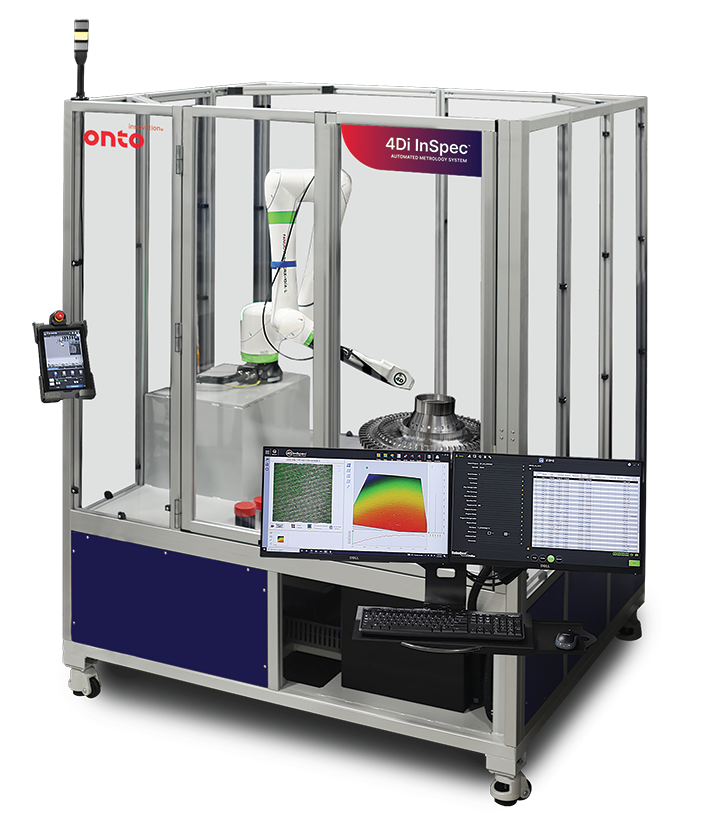
The 4Di InSpec Automated Measurement System is a non-contact optical surface gauge, either the 4D InSpec or 4D InSpec XL, integrated with a choice of collaborative robots, an optional rotary table and a safety cell for rapid production inspection.
This fully automated 3D optical system can measure dozens of edge break features, chamfers, and radii in minutes, vastly improving throughput and driving down inspection costs.
Designed as a turnkey cell for quality control, it is ideal for precision machined components such as turbine blades and rotors, air foils, high pressure compressor blades, blisks and dovetails. The high resolution system can measure in any orientation, on curved surfaces, over large and complex geometries, and in tight spaces or blind locations.
The 4Di InSpec AMS accurately captures complex feature dimensions, enabling more precise part disposition. Its rapid measurement capabilities reduce inspection queuing times, while the ability to measure at multiple locations in the same timeframe ensures part quality.
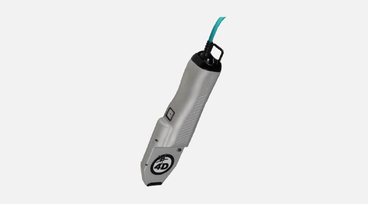
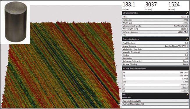

The 4Di InSpec surface gauge is a ground-breaking 3D optical gauge that enables high-resolution, non-contact surface defect and feature measurements right on the shop floor.
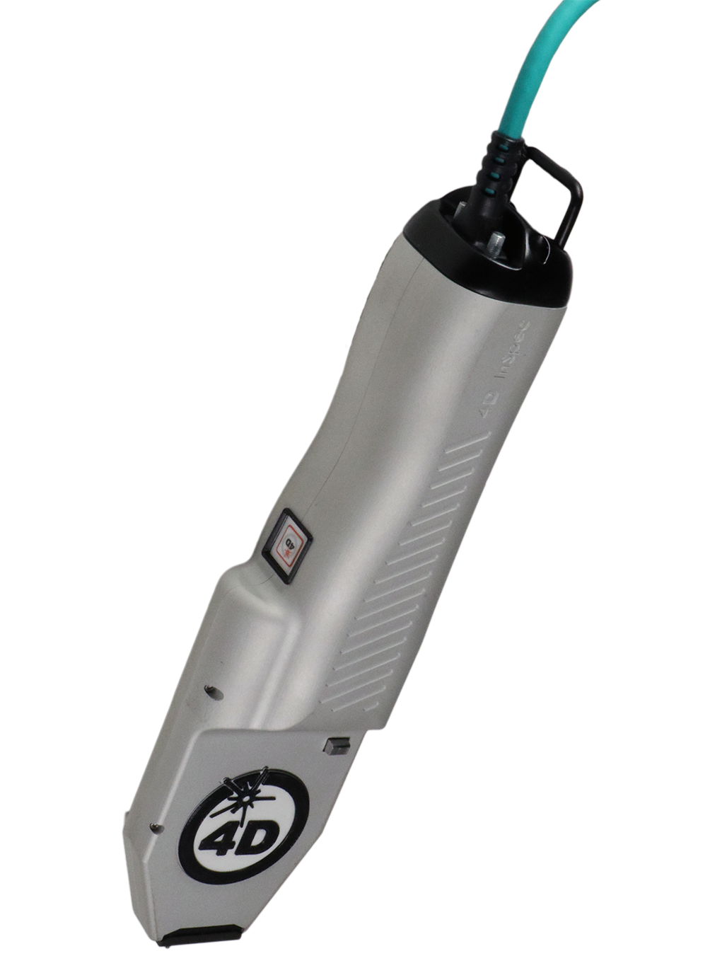
The 4Di InSpec optical surface gauge is the first handheld precision instrument designed for non-contact surface defect measurement. With micrometer-level resolution, portability, affordability and ease-of-use, the 4Di InSpec surface gauge brings high resolution 3D surface measurement where it’s needed: on the factory floor, in machine shops, and in field service applications.
This surface gauge provides 3D surface measurements to instantly quantify defects and features up to 100 mils (2,540 micrometers) deep. Without the need for replication, it can measure large components of varying complex geometries directly. It is adaptable for handheld use, workstation setups, or robotic operation with optional accessories to meet specific customer challenges.
Even with its incredible precision and extensive analysis capabilities, its ease of use allows non-experts to take measurements after just minutes of training.

The PrecisionWoRx VX4 System is designed to provide accurate and repeatable performance through enhanced testing of the latest probe card technologies with tighter pitches, smaller pads and higher pin counts.
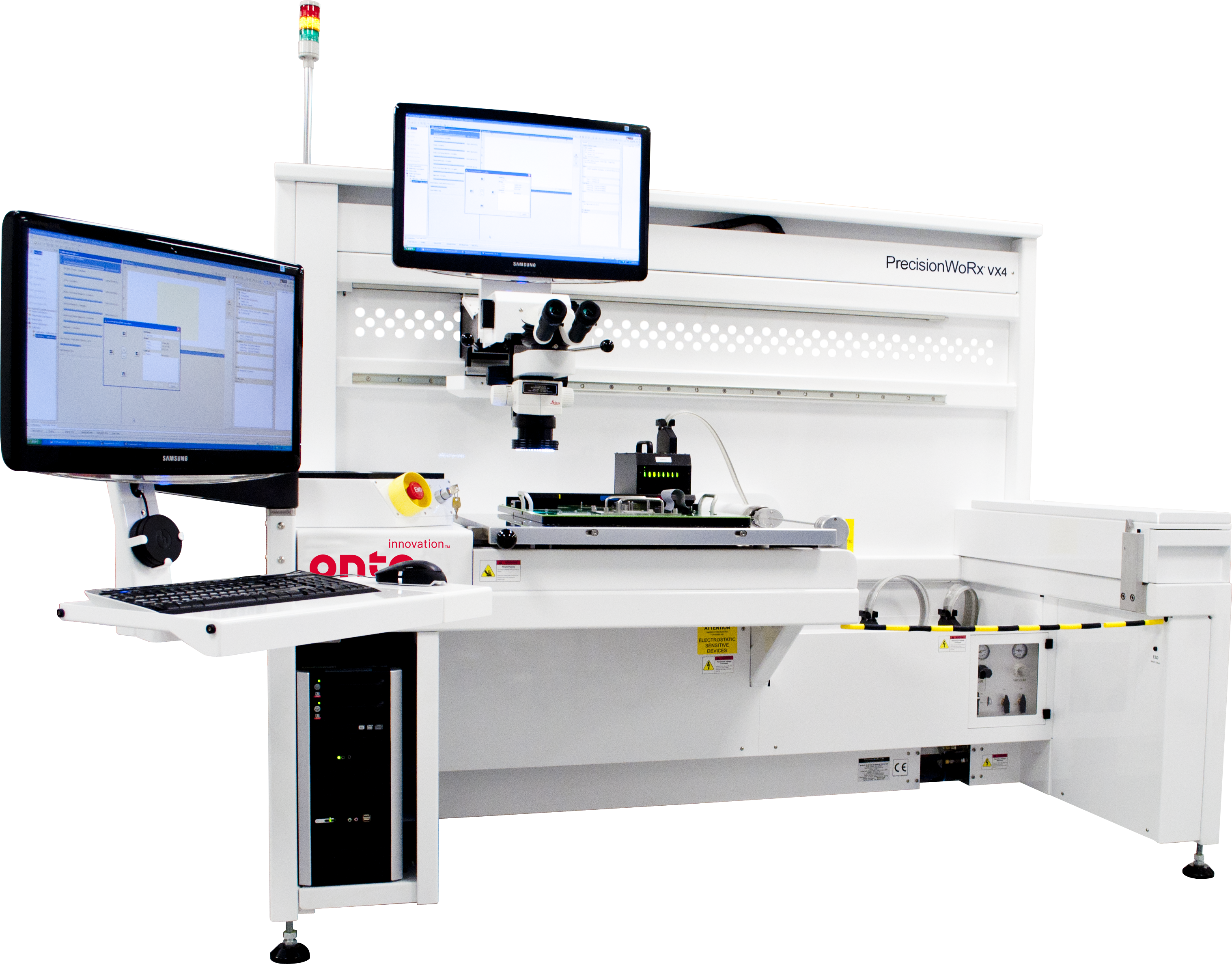
The PrecisionWoRx VX4 System gives test facilities and probe card manufacturers the ability to confidently test tighter pitches and smaller probe tips. The system can be configured to meet specific requirements for a variety of probe card technologies. For processes using cards with very small probe tips, the system’s high-resolution optics deliver a detailed field-of-view for high accuracy and repeatability. Proprietary image-processing recipes control over 30 imaging parameters for enhanced testing of most probe tip geometries in use today.
The PrecisionWoRx VX4 System improves overall cost of ownership with faster test times for common tests, including leakage, planarity, alignment, contact resistance, probe force and wire checker. Its sophisticated electrical discharge management capability maintains 1-volt continuity to the probe during electrical testing. Productivity-enhanced routines for automated testing of failed probes and a wide variety of checkplates suit an extensive range of process and technology requirements. The system provides support for the most complex probe card technologies.

As your partner for innovative solutions, we’re always here for you.
Discover how our cutting-edge semiconductor solutions are engineered to meet your most complex challenges: delivering performance, reliability and innovation where it matters most.
"*" indicates required fields