
Discover® Defect Software
Integrated defect management system that works seamlessly with Onto tools and your entire enterprise, bringing data together for greater visibility and cleaner operation.

From consumer products to industrial applications, augmented reality (AR)/mixed reality (MR) technology is one of the most innovative interactive technologies on the market today.

Sept 2 — Sept 4, 2026
Onto Innovation is a proud exhibitor at SEMICON Taiwan.
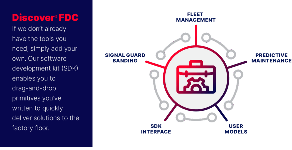
Discover FDC software is part of a robust data management suite, serving as the ideal gateway to digital transformation and unlocking Industry 4.0 best practices for impactful results.
Discover FDC software transforms tool sensor data into actionable insights. It empowers manufacturers to optimize fab efficiency, scaling seamlessly to high-volume manufacturing while reducing tool downtime by detecting anomalies early. With its diverse set of flexible controls and real-time data analysis, Discover FDC software enhances productivity, improves cycle time and increases equipment availability (OEE). Its user-friendly interface integrates advanced process control, allowing engineers to pinpoint issues and bring equipment online faster. Proven across processes and operational modules, it eliminates wasted time and energy by preventing idle tools and minimizing scrapped wafers. When connected to Discover Defect and Discover Yield software, Discover FDC software identifies meaningful correlations that drive even greater efficiency and production results. This robust solution redefines control, setting a new standard for achieving maximum enterprise-wide factory performance. That’s control, redefined.


As your partner for innovative solutions, we’re always here for you.
Discover how our cutting-edge semiconductor solutions are engineered to meet your most complex challenges: delivering performance, reliability and innovation where it matters most.
"*" indicates required fields
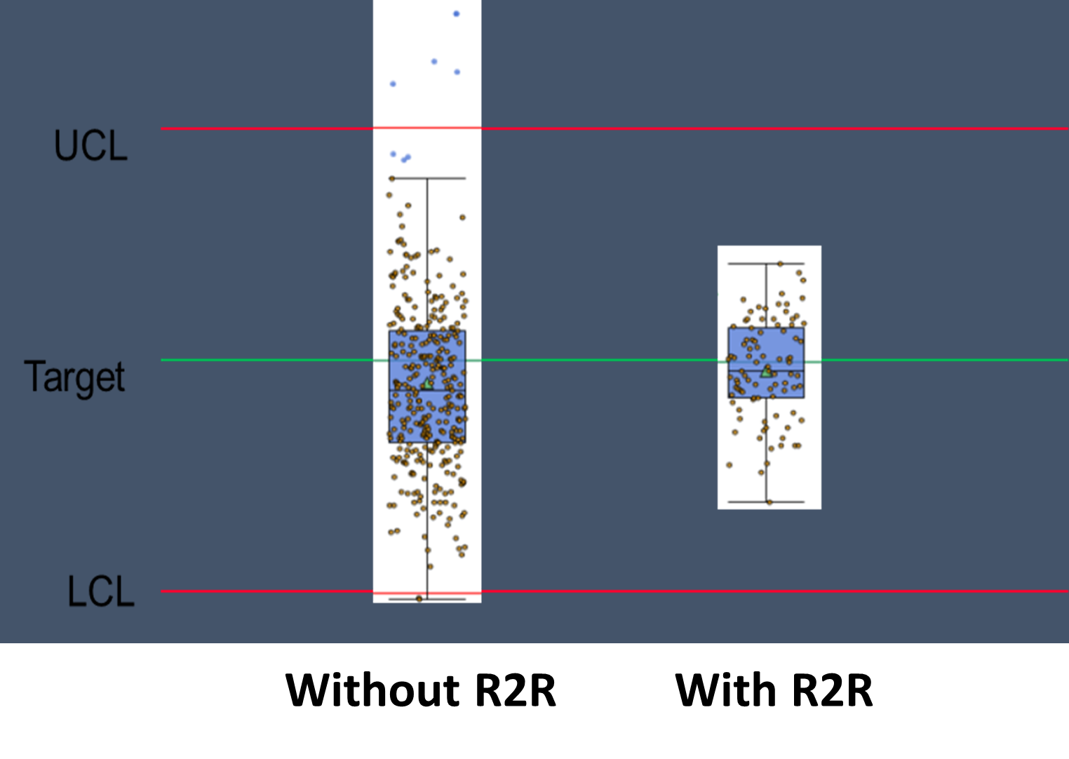
Discover Run-to-Run software boosts profits and productivity with swift deployment on any process or tool, increasing Cpk and throughput while reducing pilot wafers, engineering time and manufacturing costs.
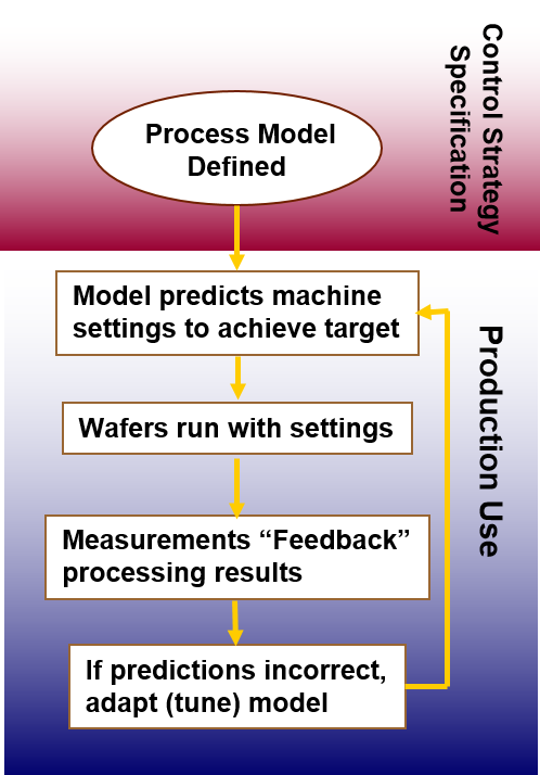
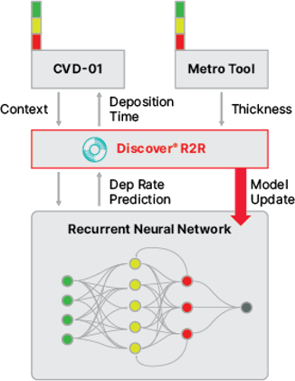
Discover Run-to-Run software is a feature-rich application that enables advanced supervisory process control, surpassing traditional statistical methods. It ensures precise process goals. For example, achieving desired thickness is possible through tailored adjustments of machine parameters like deposition duration or pressure settings. Designed for high-mix production, it allows seamless transfer of control strategies across factories for operational flexibility. Proven globally, it operates thousands of tools across hundreds of processes continuously. With its adaptable, framework-based APC solution, Discover Run-to-Run software enables rapid factory-wide deployment, delivering significant and immediate return on investment while enhancing consistency, productivity and efficiency.

As your partner for innovative solutions, we’re always here for you.
Discover how our cutting-edge semiconductor solutions are engineered to meet your most complex challenges: delivering performance, reliability and innovation where it matters most.
"*" indicates required fields
Discover Yield software is a complete yield management enterprise platform that combines parametric, defect and yield optimization with data mining and workflow development across all data sources from memory and design to assembly and packaging.
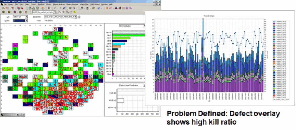
Discover Yield software helps reduce the time it takes to find root causes of yield excursions and enables manufacturers to broaden their analysis scope for better yield management.
The software includes data acquisition and integration, a development environment through workflow and scripting, and specialized analysis algorithms to identify domain-specific issues, such as data mining, spatial anomalies, wafer processing sequence problems, commonality of effects, system and random yield loss, chamber matching, tool events, traceability and more. In addition, Discover Yield software provides distinct tools – principal components and multivariate analysis of variance (MANOVA) – that allow systematic, simultaneous examination of multiple variables. Discover Yield software’s database architecture for genealogy uniquely supports value chain predictive analytics.
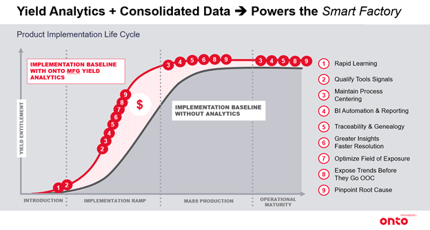
Improving baseline yield with analytics


As your partner for innovative solutions, we’re always here for you.
Discover how our cutting-edge semiconductor solutions are engineered to meet your most complex challenges: delivering performance, reliability and innovation where it matters most.
"*" indicates required fields
Discover AI software leverages high-quality data input to provide valuable insights into processes and actionable predictions for process, yield and efficiency improvements through integration with the Discover data platform.
Discover AI software is a disruptive technology that reshapes the way we approach manufacturing line control and yield analysis. It leverages the latest in machine learning and artificial intelligence to identify actionable improvements and connections in data that a human could not. The software’s optimization engine adds a powerful machine learning analytical method to an already sophisticated toolbox of process improvement applications.
By analyzing any set of conceivable inputs and outputs, Discover AI software identifies relationships and interactions that lead to positive operational changes. Easily understood visuals empower even casual users to understand what is important before making adjustments.
Discover AI software evaluates multiple models and suggests the optimal one for the data. Using machine learning, it examines interactions between in-process inputs and results for any semiconductor product family and recommends changes to in-process targets. Licensed as a service, it enables users to leverage an on-demand infrastructure to apply easily understood workflows for complex analytics without the overhead.
As your partner for innovative solutions, we’re always here for you.
Discover how our cutting-edge semiconductor solutions are engineered to meet your most complex challenges: delivering performance, reliability and innovation where it matters most.
"*" indicates required fields
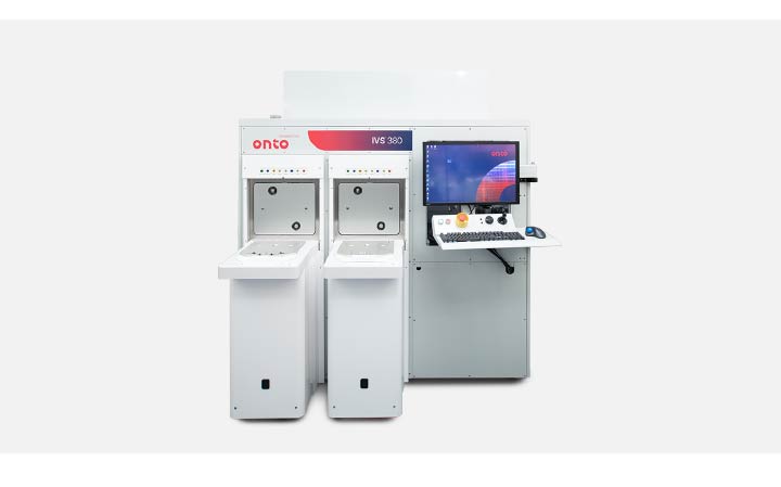
The IVS 380 System delivers overlay, CD and z-height metrology for advanced packaging, power, compound semi and MEMS, offering world class performance and flexibility to accommodate substrates of different sizes and thickness without hardware changes.
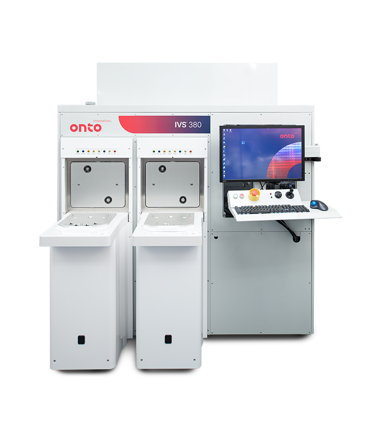
The IVS 380 is an optical overlay, CD & z-height metrology system designed for high volume manufacturing, with SMIF (200mm substrate) or FOUP (300mm substrate) load ports compatibility. It handles various substrates for advanced packaging, including Si, glass and CCL, and accommodates sizes of 200mm and 300mm.
Building on the IVS family’s 40 years of experience in CMOS, MEMS and compound semiconductor applications, the IVS 380 system possesses the versatility to tackle overlay, CD and z-height measurements for diverse substrates and layers. It measures critical dimensions in the xy plane and the vertical z-heights of features like RDL metal lines, posts and bumps. The optics enable focus on mostly transparent materials such as photoresists and rough surfaces such as electroplated copper.
Enter your information below and we’ll send you a unique passcode to view our IVS 3D Demo.
As your partner for innovative solutions, we’re always here for you.
Discover how our cutting-edge semiconductor solutions are engineered to meet your most complex challenges: delivering performance, reliability and innovation where it matters most.
"*" indicates required fields
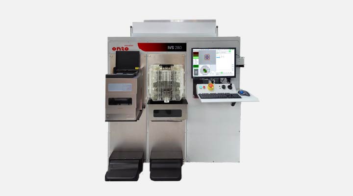
The IVS 280 system delivers overlay, CD and z-height metrology for 100mm-200mm wafers. It is designed to meet the challenging requirements of power, compound semi and MEMS segments.
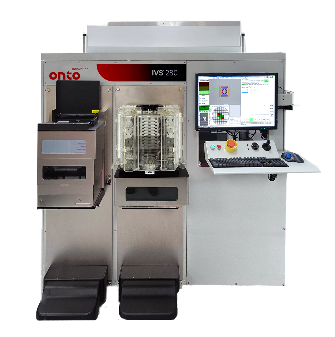
The IVS 280 system has been designed for ultimate precision, tool induced shift (TIS) and throughput for 100mm to 200mm wafers, with a mean time between failure (MTBF) > 2,000 hours. The IVS 280 system provides the same capability in a system designed for overhead track handling with full capability per SEMI® standards.
Flexibility is key in compound semiconductor processes, accommodating various wafer sizes, thicknesses, and compositions, including versatile wafer handling for Si, SiC, quartz, glass, GaAs, GaN, and LiNO3 wafers.
Its robust wafer handling and navigation system requires no operator assistance during recipe execution. The IVS 280 system enables wafer size changes without hardware alterations. Recipes and data remain stable over time. The system also supports recipe transfers from older IVS platforms like the IVS 200 and IVS 220.
The demonstrated capabilities of the IVS system to perform with high precision and solid reliability set this system apart.
Enter your information below and we’ll send you a unique passcode to view our IVS 3D Demo.
As your partner for innovative solutions, we’re always here for you.
Discover how our cutting-edge semiconductor solutions are engineered to meet your most complex challenges: delivering performance, reliability and innovation where it matters most.
"*" indicates required fields