
Atlas® V System
High performance OCD and thin film metrology for advanced GAA and memory devices.

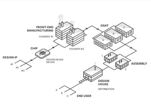
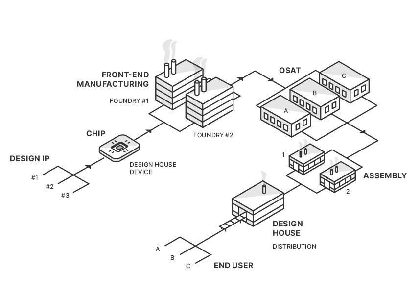
If you’ve been following the evolution of advanced packaging, you know that the industry is pushing boundaries like never before. From high-performance computing to industry-upending AI devices, the demand for smaller, faster, and more powerful chips is driving innovation at every level.

A suite of OCD modeling software and computing hardware that enables the full capability and connectivity across all Onto OCD and thin film metrology systems, including Atlas, Aspect, Iris and IMPULSE systems.
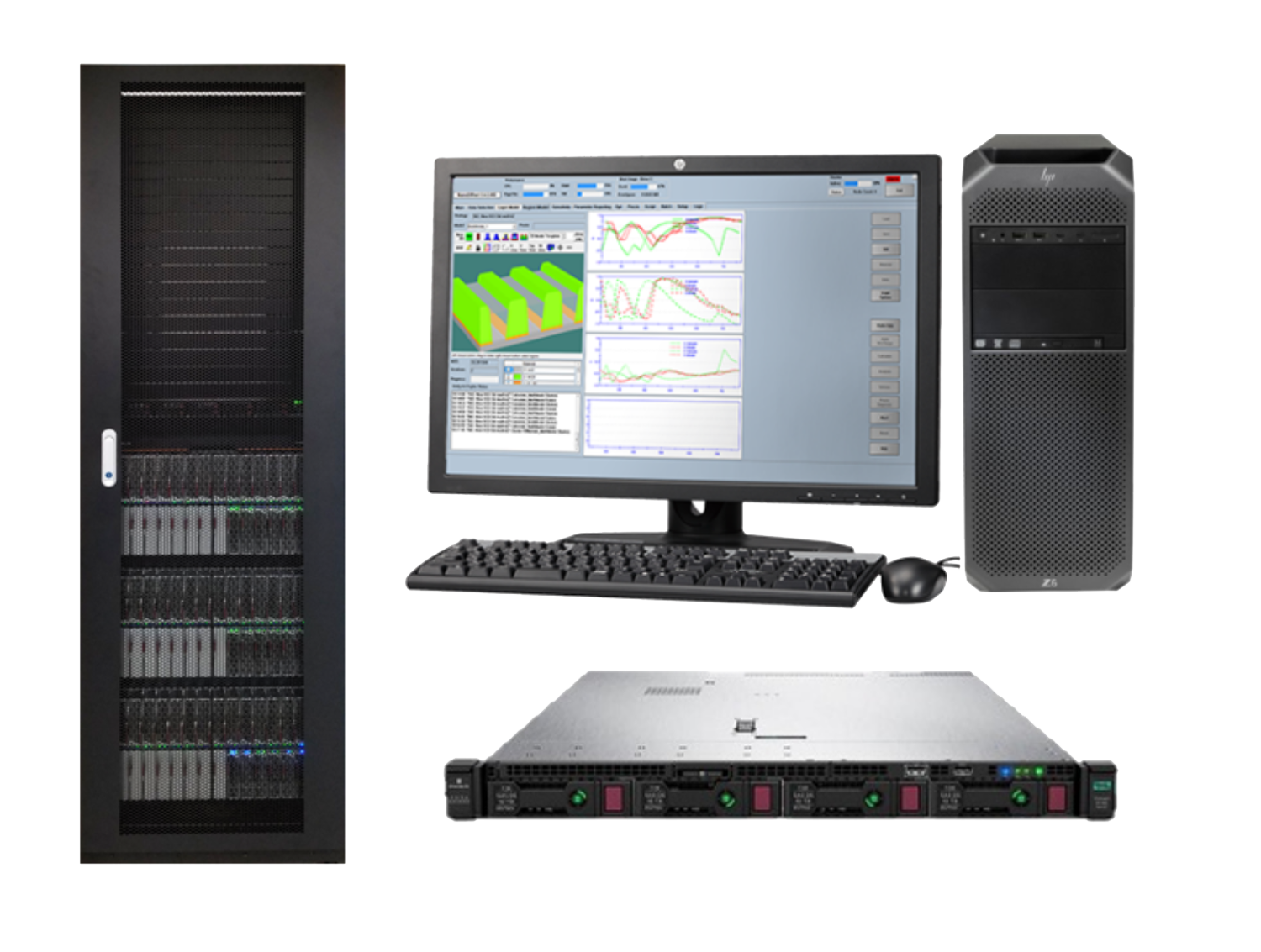
Onto Innovation’s OCD technology offers powerful modeling and computing packages to support various phases of film and OCD measurement setup, data management, and fleet management. These capabilities include model building, runtime data analysis, system calibration, data analytics, data connectivity and management, spectrum management and fleet matching.
Onto OCD solutions consist of several modeling and computing components, including Ai Diffract™ modeling software, runtime onboard computer, offline modeler, offline model building clusters, and recipe & data management server. Each component seamlessly extends OCD capabilities to Onto’s standalone and integrated metrology systems, providing end-to-end capabilities from offline recipe support and development to fab-wide networking and connectivity for easy fleet management.
Ai Diffract software is a powerful modeling, visualization and analysis software with an intuitive 3D modeling interface to simplify the building and visualization of today’s most complex semiconductor devices. It offers OCD modeling and advanced machine learning capabilities, next-generation real-time regression, offline sensitivity analysis tools and comprehensive GUI and structure input for true multi-variant modeling. Ai Diffract software’s proprietary fitting algorithms enable fast and accurate calculations for signal processing, helping ensure high fidelity model-based measurements. Automation features for spectral fitting, recipe optimization, and sensitivity analysis offer great user productivity. The first-in-market AI-guided engine synergizes physics-based modeling and machine learning to deliver the most robust solution with quick time to solution.
Ai Diffract Modeler is the offline analytical engine that allows users to create and edit recipes offline. It supports multiple users and can connect to Ai Diffract cluster for high intensity computing.
Ai Diffract Onboard is the on-tool runtime engine that maximizes tool throughput for complex use cases. It ensures rapid analysis without interfering with system operation or impacting throughput.
Ai Diffract Cluster is an enterprise scale computing server deployed for offline recipe development or in-line real-time regression. Optimized to support the workload of Ai Diffract software analysis, it scales based on fleet size, recipe numbers, and computing intensity.
Recipe Distribution Server (RDS) / Nexus Servers is a fab-wide networking and server system for fleet management and connectivity. RDS/Nexus servers provide connectivity and support to Ai Diffract recipe management and distribution, data/spectrum feed-forward and feedback, spectrum management, and fleet management.


As your partner for innovative solutions, we’re always here for you.
Discover how our cutting-edge semiconductor solutions are engineered to meet your most complex challenges: delivering performance, reliability and innovation where it matters most.
"*" indicates required fields
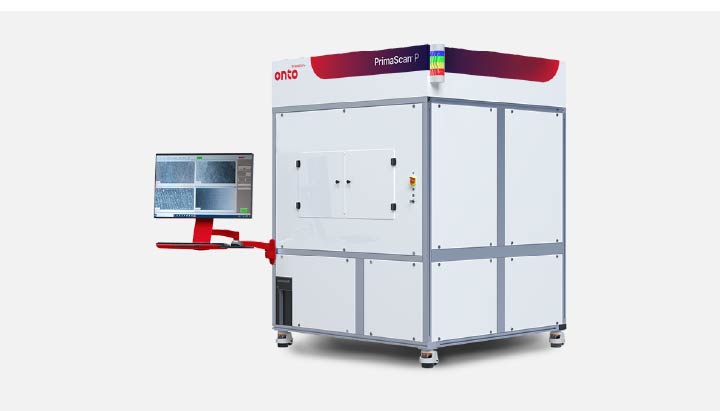
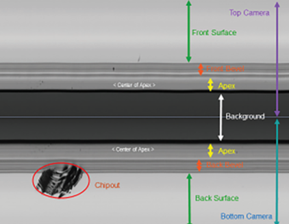
The PrimaScan wafer defect inspection system delivers a flexible, high sensitivity solution at the lowest cost of ownership per pass.
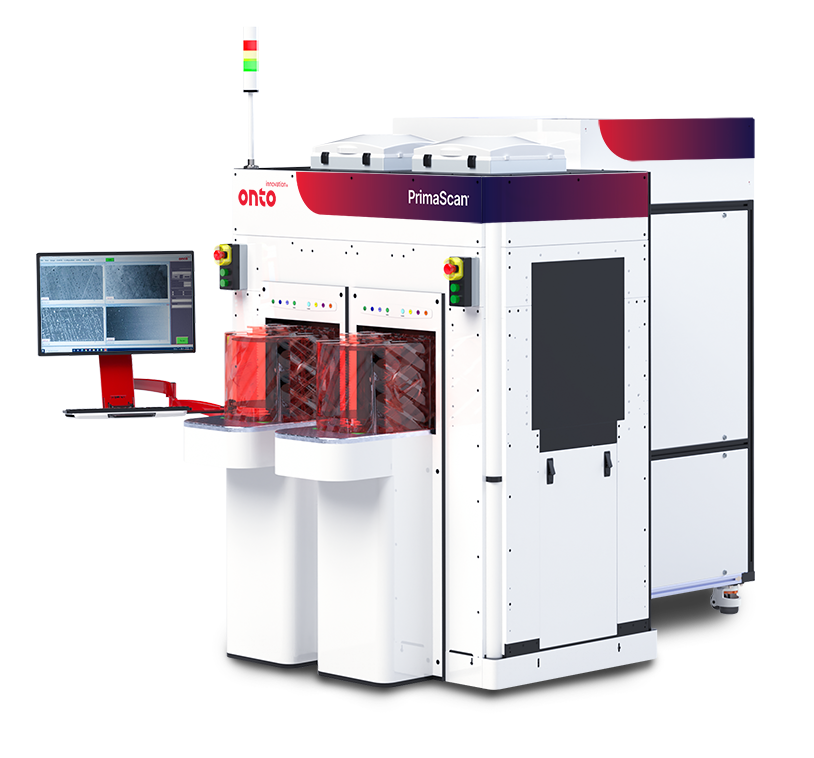
The PrimaScan system utilizes laser scatterometry and imaging techniques leveraging proprietary optics and sensing technologies for reliable inspection of nanometer sized defects on a variety of opaque and transparent/semi-transparent substrates suitable for either R&D or high-volume manufacturing environments. With multiple detection channels, the system can detect, measure, characterize and image surface particles, scratches, pits, bumps, surface contamination, film or bulk wafer stress, voids/inclusions, including chips and cracks at the wafer edge.
The PrimaScan system addresses challenges in both incoming wafer quality control and in inline process monitoring. Capable of handling multiple substrate materials, it uniquely addresses inline process defect and contamination monitoring in wafer-based production environments.
Designed with versatility in mind the PrimaScan system can handle a variety of wafer sizes and substrate types

As your partner for innovative solutions, we’re always here for you.
Discover how our cutting-edge semiconductor solutions are engineered to meet your most complex challenges: delivering performance, reliability and innovation where it matters most.
"*" indicates required fields
Yield Optimizer software is part of a comprehensive next-level data management portfolio. It reimagines manufacturing line control and analytics to explore the impact of previously invisible factors in day-to-day factory operation.
Yield Optimizer software is the next incarnation of analytics on the evolutionary scale. The software’s disruptive technology analyzes relationships between multivariant data and their complex interactions. By examining any set of conceivable inputs and outputs, Yield Optimizer software identifies the relationships and interactions that lead to positive operational changes. Easily understood visuals empower even casual users to understand what is important before making adjustments.
Yield Optimizer software evaluates multiple models and suggests the best one for the data. Using machine learning, it examines the interactions between in-process metrology readings and end-of-line test results for any semiconductor product family and recommends changes to the in-process metrology targets. When licensed as a service, it enables users to leverage an on-demand infrastructure to apply easily understood workflows for complex analytics without the overhead.
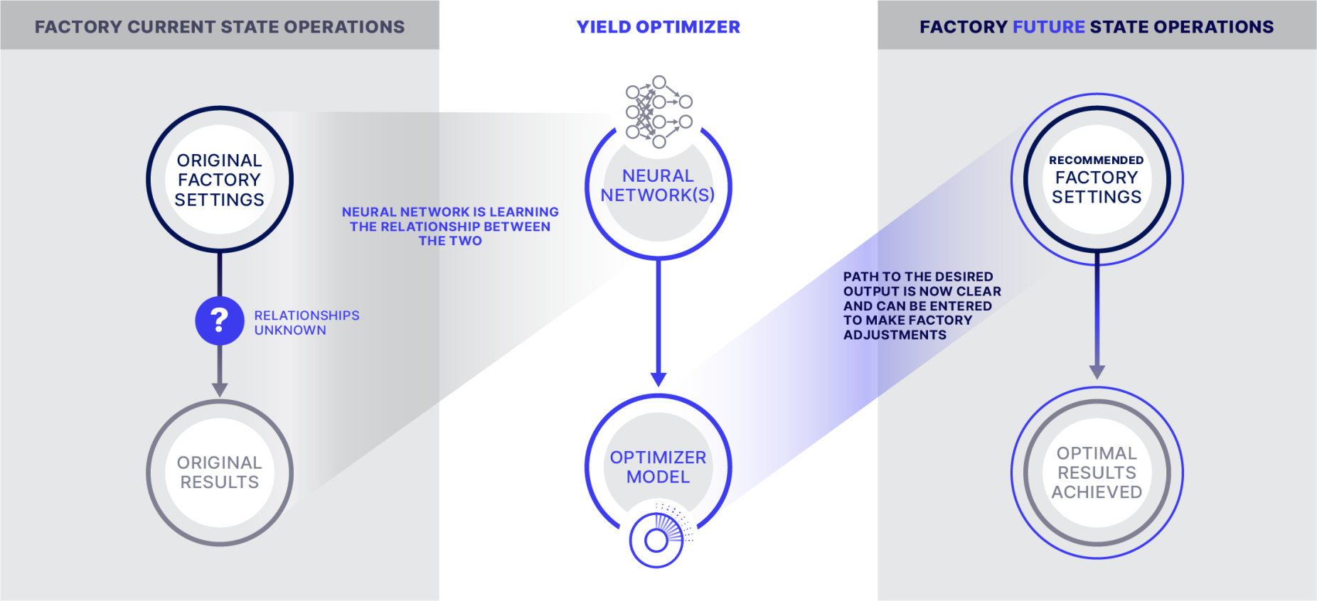
Neural networks model today’s data to achieve tomorrow’s in-line targets

Users across the fab benefit from Yield Optimizer software’s easy-to-apply analytics


As your partner for innovative solutions, we’re always here for you.
Discover how our cutting-edge semiconductor solutions are engineered to meet your most complex challenges: delivering performance, reliability and innovation where it matters most.
"*" indicates required fields
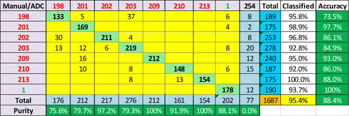
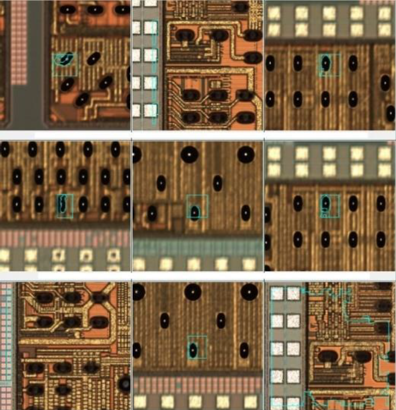
TrueADC software enhances defect classification accuracy and efficiency by combining deep learning, real-world defect modeling, and intuitive workflows—reducing manual review and improving decision-making across all wafers and surfaces.
TrueADC software sets a new standard in defect classification by combining advanced analytics with intuitive usability. Seamlessly integrated with Onto Innovation’s AOI tools and Discover platforms, TrueADC software enhances inspection value through a proprietary hybrid decision-making process across all wafers and surfaces.
With over 70% reduction in manual review, TrueADC software intelligently flags low-confidence defects as “unknown” to avoid misclassification. Its dynamic defect library method uses real defect examples—unlike traditional ADCs that rely on approximations—delivering more accurate and efficient results.
Supporting adder, repeater, SPR codes, and region-of-interest data, it enables precise tool sampling and binning. Operators can quickly classify new defects without altering recipes, while the software’s multi-engine mode leverages deep learning to reduce overkill and underkill.
From model development to identifying hard-to-isolate defects, TrueADC software empowers engineers with greater clarity, control, and confidence.

As your partner for innovative solutions, we’re always here for you.
Discover how our cutting-edge semiconductor solutions are engineered to meet your most complex challenges: delivering performance, reliability and innovation where it matters most.
"*" indicates required fields
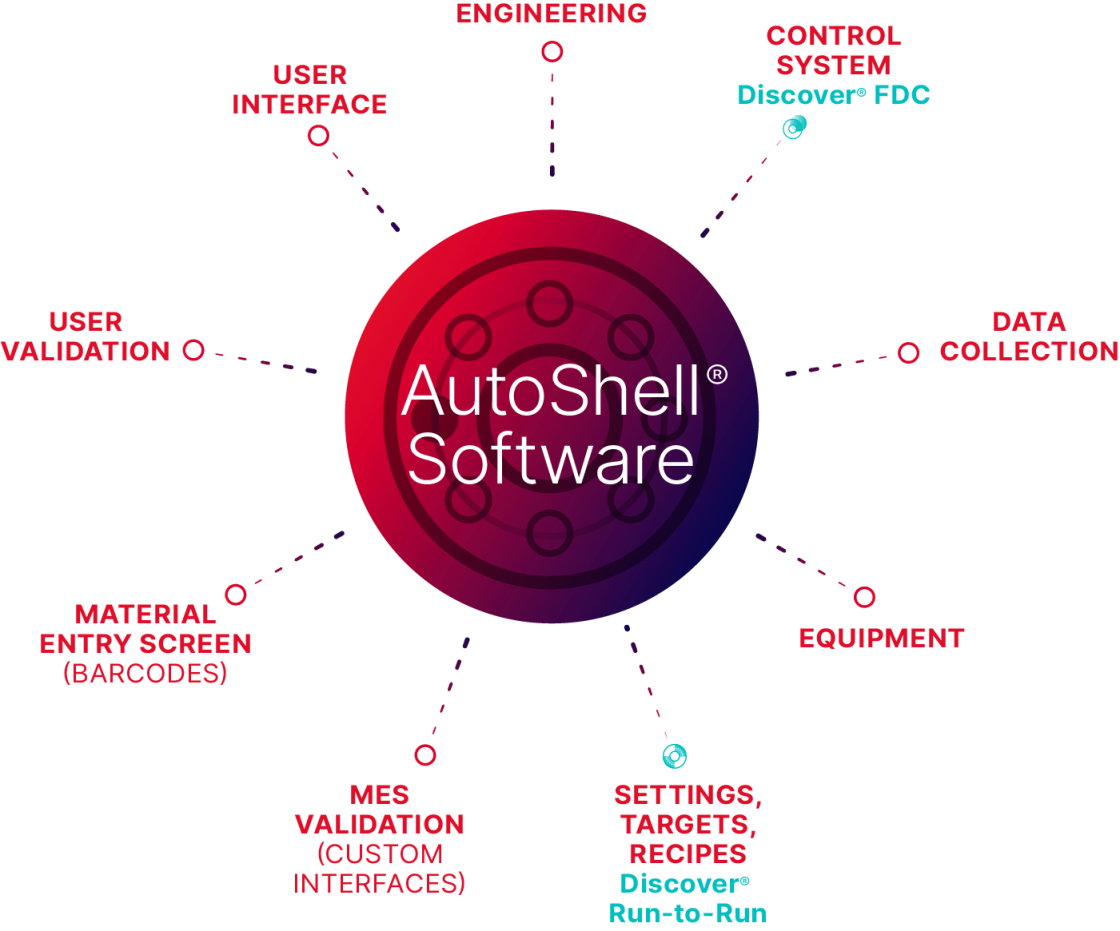
AutoShell software accelerates Industry 4.0 adoption by connecting multiple data sources throughout the fab in a single platform.
In a fast-changing industry, AutoShell software ensures competitiveness by seamlessly connecting systems, equipment and people in the factory. Its reliability and uptime make it essential for digital transformation.
AutoShell software unifies products, processes, equipment, stakeholders and facilities through versatile communication protocols across factory networks, optimizing limited IT resources. Its gateway, data acquisition tools, automation suite and multilingual development kit enable efficient data management and communication.
With over 10,000 systems across 500+ product types, AutoShell software empowers customers to execute factory operations without interruption, driving productivity and adaptability. It isn’t just software—it’s the backbone of the future-ready factory.

As your partner for innovative solutions, we’re always here for you.
Discover how our cutting-edge semiconductor solutions are engineered to meet your most complex challenges: delivering performance, reliability and innovation where it matters most.
"*" indicates required fields
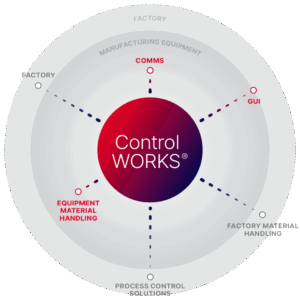
ControlWORKS software manages equipment-level material handling, factory communication, advanced scheduling and UI development through a comprehensive single machine control platform. This software increases product development efficiency and reduces time to market.
Next-generation technology nodes are advancing faster than process equipment development, challenging manufacturers to shorten product timelines. The ControlWORKS platform streamlines tool automation, allowing engineers to focus on innovation that drives market adoption. Its Object-Oriented Architecture supports swift development of diverse equipment types and processes. The Reusable Class Library enhances exception handling, communication and multitasking. Its SEMI® software compliant design adheres to industry standards (SECS/GEM, EDA, 300mm) and functions across multiple operating systems, including Windows, Linux and VxWorks. Together, these features empower efficient and scalable manufacturing, while ensuring compatibility with industry norms.
As your partner for innovative solutions, we’re always here for you.
Discover how our cutting-edge semiconductor solutions are engineered to meet your most complex challenges: delivering performance, reliability and innovation where it matters most.
"*" indicates required fields