FAaST® Digital SPV System
The FAaST Digital SPV system provides a fast, non-contact, and preparation-free method for full wafer imaging of contamination in silicon. High resolution maps of diffusion length and iron (Fe) concentration are generated in minutes, setting the industry standard for precision and sensitivity in Fe contamination control, reaching the E7 cm-3 range.
Product Overview
There is no disputing the detrimental effect of metallic contamination on the integrity of the critical gate oxide used in integrated circuits. During high temperature processing, contamination in the silicon wafer often precipitates at the Si/dielectric interface or segregates into the dielectric—both scenarios can cause premature device failure and reduced yield. As device dimensions shrink, the tolerance for contamination decreases, requiring ever-lower background levels of metals like iron (Fe). Over the past 25 years, the IC industry has reduced typical Fe concentrations by more than three orders of magnitude, yet further reduction is essential, especially for applications like CMOS image sensors.
The FAaST Digital SPV system addresses this challenge with industry-leading sensitivity and speed. It provides a fast, non-contact, and preparation-free method for full-wafer imaging of contamination. High-resolution maps of minority carrier diffusion length and Fe concentration are generated in minutes, enabling fabs to detect and control contamination at levels as low as the E7 cm⁻³ range.

Figure 1. Typical background Fe concentration in new IC Fablines (blue) and the state-of-the-art SPV detection limit (red)
Applications
- Ingot qualification
- Outgoing / incoming polished wafers
- Epitaxy
- Cleaning
- Diffusion furnace monitoring
- Rapid thermal anneal
Featured Markets
Do you have a FAaST Digital SPV system question? Let’s talk!
As your partner for innovative solutions, we’re always here for you.
Discover how our cutting-edge semiconductor solutions are engineered to meet your most complex challenges: delivering performance, reliability and innovation where it matters most.
Let’s Talk
"*" indicates required fields
CnCV® System
The CnCV system enables wafer-level characterization of WBG materials without test device fabrication, reducing time and cost. As a mercury-free alternative to MCV, it eliminates contamination concerns. The enhanced Kinetic CV mode with UV-assisted corona charge neutralization achieves high throughput and precision for fast, reliable process control.
Product Overview
The CnCV system utilizes a novel constant surface potential corona charging, which enables the precision required over a large voltage range. The patented technology includes charge- and photo-assisted modes, especially suited for speed and precision on WBG materials and structures, including SiC, Ga2O3, GaN, and AlGaN/GaN HEMT. Additionally, Corona-Kelvin characterization includes electrical properties of dielectrics and interfaces of films on SiC and GaN epi layers. An automated top-side edge contact (TSEC) is also available enabling characterization of WBG on insulating/semi-insulating substrates. Automated bias-temperature stress (BTS) measurements are also available with the CnCV system, providing a fast, noncontact way to quantify the reliability of passivated SiC and GaN.
Beyond typical CV type parameters, the full wafer corona approach allows for QUAD (quality, uniformity, and defect) mapping. The electrical defect imaging, QUAD-EDI, mode is especially designed for SiC. It provides a unique means for quick screening of epi electrical defectivity enabling improvement in device yield prediction.

Figure 1. QUAD-EDI Map on final metallized device wafer after Merged Schottky PiN diode fabrication identifying failed dies.
Applications
- Non-contact epi dopant depth profiling in WBG materials
- AlGaN\GaN HEMT measurements (pinch off voltage & 2DEG sheet charge)
- Dielectric and interface characterization electrical defect imaging in SiC for yield prediction
- Bias-temperature stress (BTS) instability measurements on passivated WBG materials
Featured Markets
Do you have a CnCV system question? Let’s talk!
As your partner for innovative solutions, we’re always here for you.
Discover how our cutting-edge semiconductor solutions are engineered to meet your most complex challenges: delivering performance, reliability and innovation where it matters most.
Let’s Talk
"*" indicates required fields
At some point in our lives, we have dropped a drinking glass or knocked over a glass-blown knickknack, only to watch it hit the floor and shatter into pieces. We learn from any early age that glass is fragile. But if glass is so fragile, why are manufacturers adopting glass core substrates?
Good question. And one that comes with a ready answer.
Glass is able to meet the new, denser line-space specifications—1.5µm and below—for interconnects that advanced logic nodes and advanced packages require. Two, glass core is better suited for large package sizes than organic substrates (Figure 1). And contrary to what those outside the semiconductor industry may think, glass substrate offers superior mechanical strength compared to its organic counterpart.
As it stands today, organic substrates will remain viable for advanced packages, but in the near future glass substrates might emerge as the preferred substrate for high-performance applications (Figure 1).

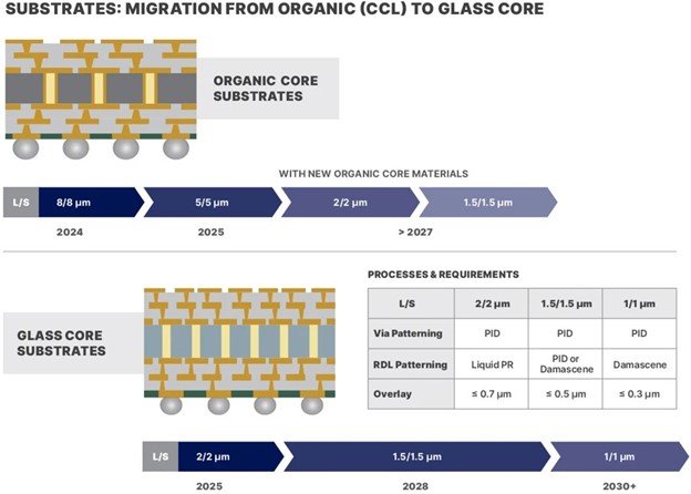
Figure 1: Roadmap for organic and glass core substrates
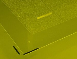
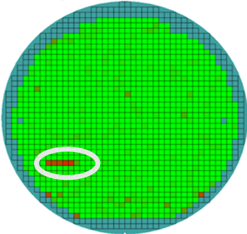
Through glass vias (TGVs) are the critical vertical electrical connections that pass through a glass substrate, and they require ultra-precise processing. Unfortunately, each step opens the process to a host of potential defects. Cracks, in particular, are problematic. A small crack early in the process has the potential to grow into a much larger, “killer” defect later in the manufacturing process that affects the performance and reliability of the end product.
These challenges are not limited to cracks, however. The position accuracy of TGVs is vital to ensure reliable electrical connections between the front and back of the glass substrate. Even slight misalignments can lead to signal integrity issues or device failure. In addition, the shape and size of the vias are another area of concern; as a result, the critical dimensions (CD) of these vias must be tightly controlled. The relationship between the top, bottom, and waist diameters of a TGV determines the taper angle and profile of the via. If the sidewall is too steep or reentrant (narrower at the bottom), it can affect the plating process, leading to incomplete metal-filled vias or voids, impacting the electrical signal performance and reliability of the final device.
As glass core substrates are growing in adoption, the TGV process is being rapidly developed, with process control challenges spanning the entire process. Proper process control includes ensuring the cleanliness of the incoming bare glass, determining the thickness uniformity of the glass, and measuring critical dimensions after each process step, from laser modification and chemical etching to metal filling. Control for each of these is critical to maintaining the integrity of the final product and optimizing yields.
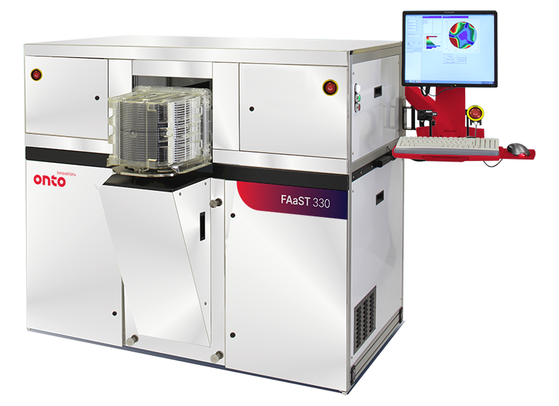
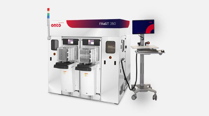
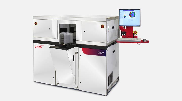
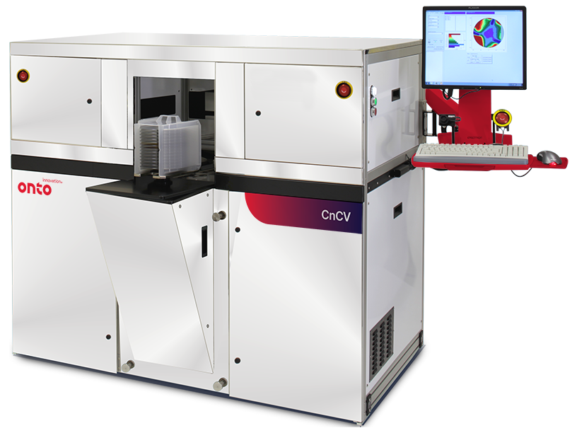
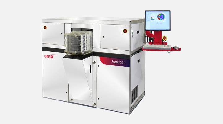
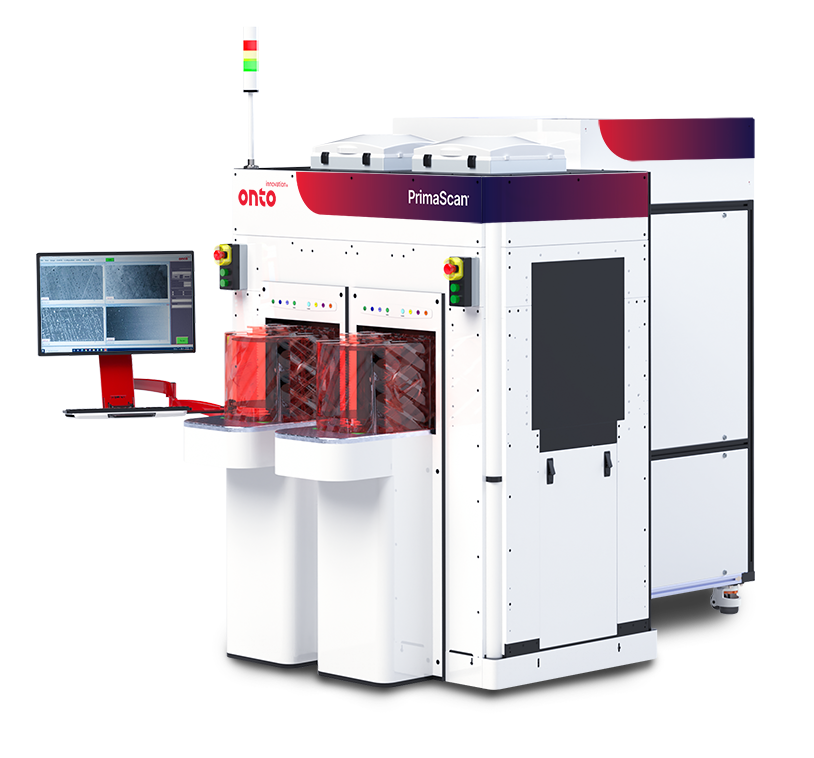
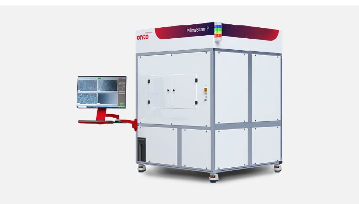
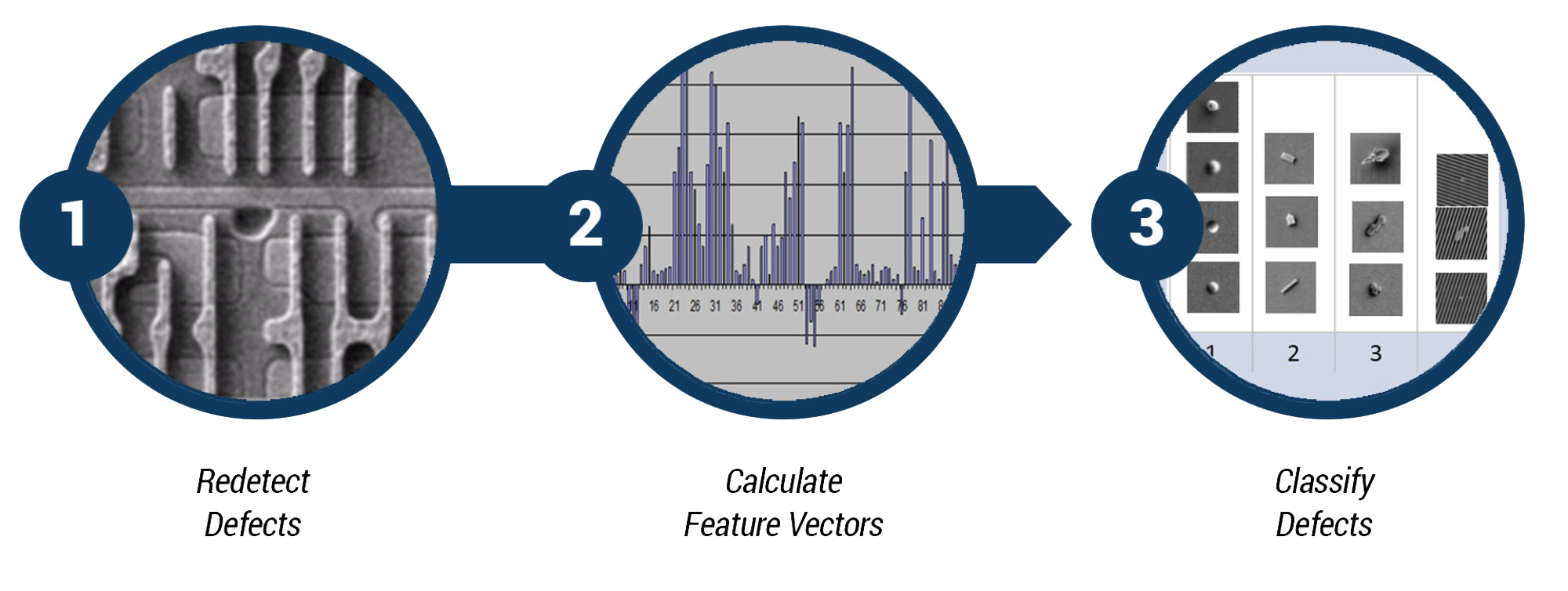
In this blog we will explore how a combination of metrology and inspection tools, along with software analytics, can be used to help develop TGVs, beginning with the inspection of the bare glass, continuing with measuring the thickness of the glass, and following with measuring the CD of the vias themselves.
Bare Glass, Glass Thickness, and Critical Dimensions
Before the TGV fabrication process even starts, it is important make sure the glass panel is free of defects (Figure 2). After all, you do not want to start off with a panel that already has an inclusion defect or crack. By using laser-based scanning and imaging optics and sensing technologies, manufacturers can reliably inspect bare glass for nanometer-sized defects, like particles, scratches, pits, and stains.

Figure 2: Glass panel with TGV.
It is also necessary to measure the thickness of the glass before starting the TGV process. Thickness uniformity across the glass panel is key. Consider this example: let us say that the thickness of a glass panel is 400µm at one end of the panel and 300µm at the other end. While this is an extreme example, you can imagine the effect that this might have on TGV height across the panel and the disastrous effect it would have on the performance of any device made from this glass substrate.
While inspecting the glass and measuring glass thickness before manufacturing begins is of considerable importance, there are a number of specific process steps throughout the TGV fabrication and metallization process where CD metrology and defect inspection are vital.
After the laser modification and etching process, manufacturers need to measure CD at the top of the via, the waist of the via, and bottom of the via;. A high-resolution, high-throughput optical panel inspection and metrology system can be used to measure these parameters for every single TGV on the panel, enabling precise monitoring of the etching process. In addition, the ability to detect defects such as incomplete etching, microcracks along individual TGV, larger cracks between multiple TGVs, and dimples and dents on the glass surface are crucial for process optimization.
In the metallization and planarization step, inspection systems can continue to monitor for defects such as residues, over/under plating, excess/insufficient polishing, and surface roughness, each of which could affect the overall electrical performance.
With millions of TGV on a panel, the ability to analyze a large quantity of inspection and metrology data within a short time period is a significant capability. The use of yield management software can shorten the time for analysis, identify systematic defects, and correlate process parameters with yield outcomes.
Conclusion
The adoption of glass core for IC substrate is currently at the starting point of what could be considerable market growth. By 2030 glass core substrate revenue is projected to grow to $275 million, according to best case scenario results from the . With the right tools on hand, manufacturers will be equipped to meet the rising demand for glass core substrates.
However, unlocking the full potential of glass core substrates and TGVs are not just about having tools; it is about using them in concert to build a process that is robust, repeatable, and yield optimized. As the adoption of glass as a substrate accelerates, manufacturers that invest in comprehensive process insight will be the ones that lead.
Monita Pau is Strategic and Product Marketing Director, Advanced Packaging, at Onto Innovation.
You Have a Challenge? Let’s talk.
We’d love to connect with you.
Looking to learn more about our innovative solutions and capabilities? Our team of experts is ready to assist you. Reach out today and let’s starts a conversation about how we can help you achieve your goals.
Let’s Talk
"*" indicates required fields
PrimaScan™ System
The PrimaScan wafer defect inspection system delivers a flexible, high sensitivity solution at the lowest cost of ownership per pass.
Product Overview
The PrimaScan system utilizes laser scatterometry and imaging techniques leveraging proprietary optics and sensing technologies for reliable inspection of nanometer sized defects on a variety of opaque and transparent/semi-transparent substrates suitable for either R&D or high-volume manufacturing environments. With multiple detection channels, the system can detect, measure, characterize and image surface particles, scratches, pits, bumps, surface contamination, film or bulk wafer stress, voids/inclusions, including chips and cracks at the wafer edge.
The PrimaScan system addresses challenges in both incoming wafer quality control and in inline process monitoring. Capable of handling multiple substrate materials, it uniquely addresses inline process defect and contamination monitoring in wafer-based production environments.
Designed with versatility in mind the PrimaScan system can handle a variety of wafer sizes and substrate types
Applications
- Opaque or transparent wafer incoming quality (ICQ) inspection
- Process monitor wafer particle and contamination inspection
- Unpatterned blanket photoresist, dielectric or metallic coated wafer defect inspection
- Subsurface defectivity inspection for transparent and semi-transparent films and substrates
- Glass carrier wafer defect and contamination inspection for advanced packaging
- Glass wafer defect and contamination inspection for microfluidics, microlens arrays for AR/VR/MR, flat optics, etc.
Do you have a PrimaScan system question? Let’s talk!
As your partner for innovative solutions, we’re always here for you.
Discover how our cutting-edge semiconductor solutions are engineered to meet your most complex challenges: delivering performance, reliability and innovation where it matters most.
Let’s Talk
"*" indicates required fields
Yield Optimizer™ Software
Yield Optimizer software is part of a comprehensive next-level data management portfolio. It reimagines manufacturing line control and analytics to explore the impact of previously invisible factors in day-to-day factory operation.
Product Overview
Yield Optimizer software is the next incarnation of analytics on the evolutionary scale. The software’s disruptive technology analyzes relationships between multivariant data and their complex interactions. By examining any set of conceivable inputs and outputs, Yield Optimizer software identifies the relationships and interactions that lead to positive operational changes. Easily understood visuals empower even casual users to understand what is important before making adjustments.
Yield Optimizer software evaluates multiple models and suggests the best one for the data. Using machine learning, it examines the interactions between in-process metrology readings and end-of-line test results for any semiconductor product family and recommends changes to the in-process metrology targets. When licensed as a service, it enables users to leverage an on-demand infrastructure to apply easily understood workflows for complex analytics without the overhead.
Applications
- Yield Prediction
- Process Targeting
- Design of Experiment (DOE) Assistant
- Troubleshooting

Neural networks model today’s data to achieve tomorrow’s in-line targets

Users across the fab benefit from Yield Optimizer software’s easy-to-apply analytics
Do you have a Yield Optimizer software question? Let’s talk!
As your partner for innovative solutions, we’re always here for you.
Discover how our cutting-edge semiconductor solutions are engineered to meet your most complex challenges: delivering performance, reliability and innovation where it matters most.
Let’s Talk
"*" indicates required fields
TrueADC® Software
TrueADC software enhances defect classification accuracy and efficiency by combining deep learning, real-world defect modeling, and intuitive workflows—reducing manual review and improving decision-making across all wafers and surfaces.
Product Overview
TrueADC software sets a new standard in defect classification by combining advanced analytics with intuitive usability. Seamlessly integrated with Onto Innovation’s AOI tools and Discover platforms, TrueADC software enhances inspection value through a proprietary hybrid decision-making process across all wafers and surfaces.
With over 70% reduction in manual review, TrueADC software intelligently flags low-confidence defects as “unknown” to avoid misclassification. Its dynamic defect library method uses real defect examples—unlike traditional ADCs that rely on approximations—delivering more accurate and efficient results.
Supporting adder, repeater, SPR codes, and region-of-interest data, it enables precise tool sampling and binning. Operators can quickly classify new defects without altering recipes, while the software’s multi-engine mode leverages deep learning to reduce overkill and underkill.
From model development to identifying hard-to-isolate defects, TrueADC software empowers engineers with greater clarity, control, and confidence.
Applications
- On-tool with Onto AOI systems
- Inline defect classification
- Dynamic defect library utilization
- Support for advanced defect types
Do you have a TrueADC software question? Let’s talk!
As your partner for innovative solutions, we’re always here for you.
Discover how our cutting-edge semiconductor solutions are engineered to meet your most complex challenges: delivering performance, reliability and innovation where it matters most.
Let’s Talk
"*" indicates required fields