
Dragonfly® G3 System
Highly configurable, automated, high speed 2D inspection and 3D metrology for inline process control in advanced packaging, specialty and front-end OQA.

Specialty devices are the unsung heroes of modern life. For many in the semiconductor industry today, the spotlight is on the SiC and GaN power devices used in automotive, green energy, fast-charge consumer electronics (CE), and high-performance computing (HPC) applications.

May 5 — May 7, 2026
Onto Innovation is a proud exhibitor at SEMICON Southeast Asia.
Specialty devices are the unsung heroes of modern life. For many in the semiconductor industry today, the spotlight is on the SiC and GaN power devices used in automotive, green energy, fast-charge consumer electronics (CE), and high-performance computing (HPC) applications (Figures 1 and 2).
However, specialty devices are more than just power devices. They are a broad class of semiconductor components delivering a variety of functions across multiple industry segments, including microelectromechanical systems (MEMS) in automobiles and CE to radio frequency (RF) filters for 5G/6G communications.

Figure1: Planar SiC MOSFET and trench SiC MOSFET

Figure 2: Vertical GaN and GaN on Si high electron mobility transistor (HEMT)
Photonics are another type of specialty device making industry waves. Previously viewed as something of a dark horse in the specialty sphere, photonics have made a comeback. Today, photonics are being used for 3D sensing in multiple CE applications such as smartphone user verification and 3D imaging, automotive applications in which scanning lasers are used in advanced driver assistance systems (ADAS); and telecommunications applications where photonics have long been used as optical transceivers supporting the conversion of copper wiring to optical fiber communications in data centers. While these applications and others exist for photonics, the killer photonics application is shaping up to be co-packaged optics (CPO), which enables optical communications directly from packaged XPU devices supporting AI applications.
When it comes to the broad category of specialty devices, nearly all of them are either manufactured on or previously manufactured on 150mm or 200mm wafers. However, specialty devices are moving to larger wafer sizes, either 200mm or 300mm depending on device type.
With many specialty devices scaling to larger wafer sizes, the semiconductor industry faces new challenges in process control. After all, specialty devices are known for delivering specialized features or capabilities based on a unique process step or material that often requires a customized inspection and metrology solution.
To optimize the manufacturing process, real-time process control —powered by data analytics and software —has become an indispensable requirement in specialty device fabrication. To scale specialty technologies for high-volume manufacturing, manufacturers need integrated solutions and specialty-focused platforms offering flexibility, precision, and automation across multiple wafer sizes.
In this three-part blog series, we will begin by discussing one of the most important trends in specialty devices, the transition to larger wafer sizes and what this means for specific devices. The following blogs will focus on the challenges facing the manufacturing of specialty devices and the solutions addressing these challenges.
From Niche Applications to Mainstream Products
Originally, specialty devices were referred to as More-than-Moore devices because the use of these devices went beyond the simple node scaling of traditional CMOS devices. They also were being enabled by one or more “specialty” materials or process steps. In fact, the semiconductor industry did not start using the term “specialty devices” until these devices transitioned from niche applications to mainstream products and high-volume production.
But what exactly are the benefits of these specialty materials? Let’s consider the case of specialty power devices.
The compound semiconductors used in power specialty devices, SiC and GaN, can handle high voltages more efficiently than traditional Si. They provide the ability to switch high voltages in increasingly smaller areas and at higher speeds than their silicon-based counterparts. They do this without the elaborate cooling that would otherwise be required. As these materials scale to larger wafer sizes, they necessitate upgrades in wafer fabrication equipment, inspection, and metrology tools.
Transitioning Wafer Sizes
Specialty devices have long been the domain of 150mm and 200mm wafers, with CMOS image sensors (CIS) and power management devices being the exception. That’s all changing.
On the compound semiconductor front, the high demand for GaN-based high-power, fast-switching technologies is motivating a wafer size transition from 200mm to 300mm while SiC power devices are transitioning from 150mm to 200mm in high-volume manufacturing. In addition, photonics technologies now span wafer sizes of 150mm to 300mm, and MEMS devices are offered at 300mm.
As more specialty device technologies move into high-volume manufacturing, we can expect to see a greater demand for 300mm silicon, glass, and compound semiconductor-based wafer applications. However, this transition to larger wafer sizes introduces unique challenges for each specialty device type. These devices and their challenges include:
MEMS: Larger substrates and diverse materials (Si, glass, thick metals) require tighter process control of etch depth and CD, feature height across bowed or warped wafers, and surface roughness.
SiC Power: As SiC power moves to 200mm, inspection and metrology must expand sampling, deal with increased crystal defects, and support device architecture transitions profiling complex trench MOSFETs (e.g., top/bottom CD) without killing throughput. Insufficient sampling on larger wafers creates blind spots that hurt yield and cost of ownership.
GaN Power: Moving GaN to 300mm wafers increases within-wafer variation, requiring more measurement points and precise control of trench/HEMT critical dimensions to maintain uniform performance, while dealing with increasingly brittle and bowed or warped materials.
Photonics and CPO: Co-packaged optics require metrology tools designed for die-to-die and wafer bonding (voids, Cu dishing, film variation), sub‑micron alignment, and warpage, which affects optical coupling on larger wafers and multi‑die assemblies.
CIS: CIS stacks drive high sampling density for overlay and CD uniformity. These stacks require integrated chemical mechanical planarization metrology and analytical tools to catch excursions quickly as die counts and wafer diameters increase.
To meet these challenges and others, manufacturers need upgraded metrology and inspection tools, many of which will come from suppliers with a long-standing relationship with specialty technologies. These suppliers are best prepared to meet the wafer handling, on-wafer materials, and cost-of-ownership requirements that have become synonymous with the specialty device markets.
Conclusion
The emergence of specialty devices as a vibrant market of their own is driven by the increasing complexity and functionality of end products. Even in mature markets, such as smartphone and automotive, manufacturers continue to innovate by adding new features, which, in turn, fuels demand for additional specialty devices.
In our next blog, we will further explore the many challenges facing each type of specialty device. We hope you join us as we discuss those challenges and, in part three of our series, the solutions that are available in the specialty space today.
Christopher Haire is a marketing content specialist at Onto Innovation and a former business journalist.

We’d love to connect with you.
Looking to learn more about our innovative solutions and capabilities? Our team of experts is ready to assist you. Reach out today and let’s starts a conversation about how we can help you achieve your goals.
"*" indicates required fields
The Dragonfly G5 system is engineered for inline process control of leading-edge advanced packaging technologies. As the latest generation pattern inspection system in the Dragonfly series, it delivers unparalleled accuracy in detecting submicron defects and performing high-resolution 3D measurements.
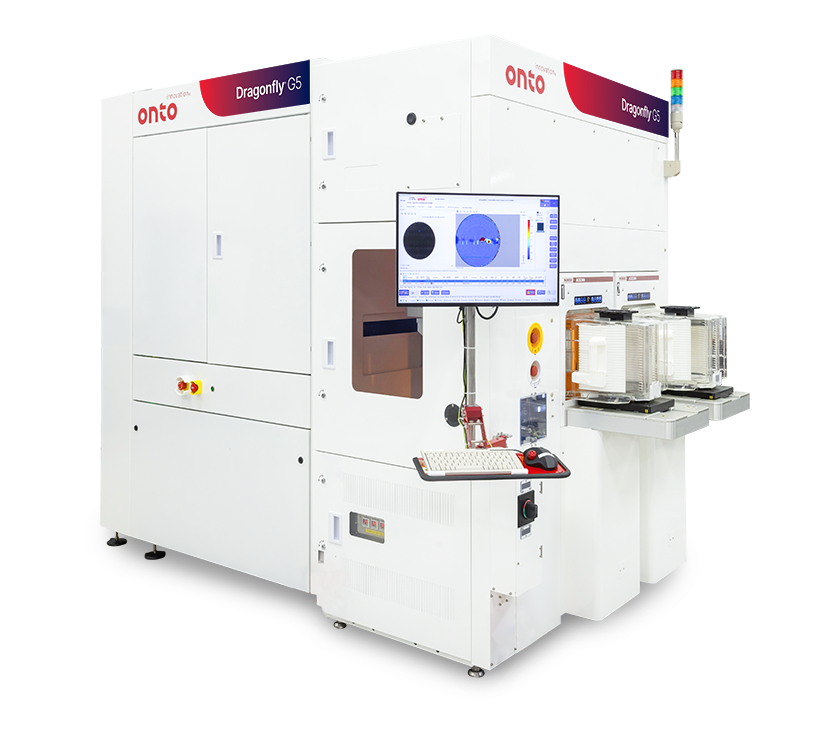
Designed to meet the demands of advanced semiconductor technologies, the Dragonfly G5 system is purpose-built to deliver high-performance, reliable inspection and metrology across complex heterogeneous integration processes. Leveraging next generation high speed line scan 2D imaging and custom-engineered objectives, the system achieves over 3X throughput improvement compared to its predecessor, with submicron sensitivity down to 150nm.
Continuing the legacy of innovation, the Dragonfly G5 system introduces a multi-angle illumination channel that significantly improves signal-to-noise ratio for faint defect detection. Combined with powerful AI-driven algorithms, it enhances both the detectability and classification of critical, yield-impacting defects–empowering fabs to maintain quality and accelerate time-to-yield.
The Dragonfly G5 system expands process control flexibility for wafer-to-wafer and die-to-wafer bonding by integrating high-speed IR imaging to detect sub-surface defects. It incorporates the latest generation of 3Di™ technology, extending bump height metrology capabilities to support next-generation microbumps essential for 3D integration. This enables additional inspection and metrology touchpoints across increasingly complex packaging architectures.


Hybrid bonding enables ultra-dense 3D memory interconnects with up to 1,000x more connections than microbumps. Achieving high yield requires stringent process control, including monitoring topography and detecting particles, cracks and voids. Measuring dishing in copper pads provides valuable insight into surface conditions. Together, these process control insights contribute to improved device reliability and performance.

As demand grows for high-performance computing (HPC) and AI-driven applications, manufacturers are turning to hybrid bonding to enable the ultra-dense 3D integration required for next-generation chip architectures. This advanced packaging technology presents significant process challenges. Surface preparation must be precisely controlled to eliminate particles, excess recess, and copper pad dishing, all of which can compromise bond quality. During pre-annealing, particle-induced gaps and wide bonding gaps can prevent proper wafer contact. Post-annealing, the formation of dielectric and metal voids introduces further risks to electrical performance and long-term reliability.

The Iris S system is a versatile platform solution for the advanced packaging and specialty market, supporting 150mm, 200mm and 300mm wafers. It provides thin and thick film, OCD and wafer bow and film stress measurements.

The IMPULSE V system helps to advance CMP processing with enhanced wavefront technology and AI-driven analytics, delivering over 2X precision improvement and faster solutions, crucial for next-gen semiconductor manufacturing demands.

The Dragonfly G5 system is engineered for inline process control of leading-edge advanced packaging technologies. As the latest generation pattern inspection system in the Dragonfly series, it delivers unparalleled accuracy in detecting submicron defects and performing high-resolution 3D measurements.

The Aspect System is a revolutionary in-line, non-destructive infrared optical critical dimension (IRCD) system measuring Z-dimension profiling of high aspect ratio structures to enable critical process control. It meets the needs of leading-edge customers with its high speed and process coverage.
As your partner for innovative solutions, we’re always here for you.
Discover how our cutting-edge semiconductor solutions are engineered to meet your most complex challenges: delivering performance, reliability and innovation where it matters most.
"*" indicates required fields
If you’ve been following the evolution of advanced packaging, you know that the industry is pushing boundaries like never before. From high-performance computing to industry-upending AI devices, the demand for smaller, faster, and more powerful chips is driving innovation at every level. One of the unsung heroes in this transformation: Glass carriers.
These carriers are becoming essential for applications involving high-bandwidth memory (HBM), 2.5D/3D integration, and chiplet architectures. During the manufacturing process, glass carriers serve as mechanical support for thin wafers and panel-level packages. Why? Glass carriers are noted for their warpage resistance, superior rigidity, and thermal stability. This combination of glass’ exceptional flatness and rigidity enables the precise placement of dies and interposers. Additionally, glass is optically transparent, which allows through-glass alignment during bonding and stacking, a critical capability for 3D integration where multiple layers must be accurately registered.
The benefits of glass carriers, however, come with several challenges, none of which should come as a surprise to anyone who has ever handled glass, whether in the fab or at home. Glass is fragile and, as such, is prone to surface defects, subsurface inclusions, and residual stress. Each of these can negatively impact die attachment quality, interconnect reliability, and die yield.
Let’s take a look at three major yield-killing culprits.
Surface defects such as particles, pits, and scratches are among the most common issues and may occur during glass carrier handling and processing, compromising the structural integrity and performance of advanced packaging assemblies (Figure 1). Particles can interfere with the bonding process, leading to poor adhesion or electrical discontinuities, while pits and scratches can propagate stress points that weaken the carrier during thermal cycling or molding.
However, subsurface inclusions and organic contamination, which are often introduced during reclaim or cleaning, pose more critical challenges. Inclusions within the glass can create localized stress concentrations, while organic residues can reduce UV transmission and cause bonding failures. These contaminants are particularly problematic in high-density interconnect environments where optical clarity and surface purity are critical.
Figure 1: Common glass carrier defects
In addition to surface and subsurface defects, residual stress represents a concern. Over time, these stress points, manifesting during thermal processing or mechanical handling, can lead to cracks or delamination, undermining the thermo-mechanical integrity of the entire package.
These potential challenges are compounded each time a glass carrier is reused in an effort to reduce overall packaging costs. Fortunately, technologies have been developed to address this obstacle. These technologies integrate AI-driven defect classification, real-time analytics, and adaptive scanning modes to maintain throughput without sacrificing accuracy, enabling manufacturers to detect surface anomalies, subsurface inclusions, and stress-induced defects with unprecedented precision.
Today’s wafer-based inspection platforms utilize laser scatterometry and imaging techniques to inspect for nanometer sized defects on a variety of opaque and transparent/semi-transparent substrates. These substrates may be suitable for either R&D or high-volume advanced IC substrate (AICS) and fan-out panel level processing (FOPLP) environments. Proprietary inspection technology with multiple detection channels and advanced signal processing algorithms is applied to achieve accuracy and reliability in glass carrier inspection.
Figure 2: Results of top (blue) and bottom (red) defect mapping.
With each channel optimized to capture unique scattering and reflection signatures, the technology differentiates between surface and subsurface defects, as well as stress-related anomalies, with remarkable accuracy. Surface particles, scratches, pits, bumps, surface contamination, film or bulk wafer stress, voids/inclusions can be detected, measured, characterized, and imaged. One of the most significant capabilities of this technology is the ability to conduct simultaneous top, bottom, and internal defect mapping, a critical need for transparent and semi-transparent substrates where defects can occur across multiple planes (Figure 2).
Beyond defect detection, Angstrom-level film thickness measurement provides precise control over surface coatings and residual layers. This capability is particularly valuable in the glass reclaim process where even minor variations in film thickness can impact UV transmission and bonding performance. By enabling accurate defect detection and grading, only glass carriers meeting stringent quality standards are returned to production.
By introducing technologies that mitigate risks by providing comprehensive defect mapping and stress analysis, manufacturers are able to maintain the mechanical and thermal integrity required for next-generation devices. This capability is especially valuable in markets such as AI devices, high-performance computing, and automotive electronics where reliability is non-negotiable. With this combination of advanced optical technology and robust algorithmic analysis, manufacturers can successfully achieve higher yields, lower costs, and greater confidence in their packaging processes.
As packaging complexity grows and the use of glass carriers increases, inspection systems that combine multi-depth defect mapping and stress analysis will become indispensable for ensuring yield and reliability in AI and HPC devices. With the explosive growth in AI-driven data centers and advanced packaging architectures, manufacturers need solutions that combine accuracy, speed, and cost efficiency. The laser-based wafer inspection technology discussed in this blog meets several glass carrier challenges head-on while enabling advanced packaging houses to maintain defect-free glass carriers in support of next-generation advanced packaging.
The future of glass carriers is clear: with the right technologies at the ready, manufacturers have the tools and the means to meet the growing needs of the AI and HPC markets.
Jason Lin is Director of Product Marketing at Onto Innovation.
We’d love to connect with you.
Looking to learn more about our innovative solutions and capabilities? Our team of experts is ready to assist you. Reach out today and let’s starts a conversation about how we can help you achieve your goals.
"*" indicates required fields
AI workloads are pushing the boundaries of compute, memory, and interconnect architectures, and to meet these goals, manufacturers are rapidly accelerating advanced logic and DRAM development. Chief among these innovations: gate-all-around (GAA) logic transistor and vertical gate (VG) DRAM, two device architectures that promise higher performance, improved power efficiency, and greater scalability.
However, the arrival of these device architectures introduces new levels of manufacturing complexity brought on by increasing high aspect ratios (HAR) and the continued shrinking of device dimensions by roughly 20–30% per generation. Fortunately, new capabilities in optical critical dimension (OCD) metrology are up to the challenge of measuring and monitoring features, such as gate profiles, film thickness, and structural uniformity, at the nanometer scale. With the right tools on hand, manufacturers can maintain high volume process control for GAA logic and VG DRAM in the AI era (Figure 1).
Figure 1: GAA (left) and vertical gate DRAM (right) present new challenges for process control (pictured above)
These new capabilities are enabling the delivery of accurate, high throughput measurements across complex 3D geometries like GAA and VG DRAM by offering smaller spot size, higher signal sensitivity, and enhanced precision.
But before we discuss these new capabilities, let’s dive deeper into the challenges of both device architectures. We’ll start with GAA.
GAA transistors feature HAR channels and stacks of multi-layered nanosheets, in some cases as thin as 10nm. The manufacturing complexity lies in controlling individual nanowires and accurately characterizing buried nanowires within three-dimensional architectures. Precise control over nanowire dimensions is critical for achieving the desired electrical performance, including higher transistor speeds and lower power consumption. As such, GAA manufacturers need metrology solutions capable of extracting unique signals with high sensitivity and precision from each layer, even those deeply buried under semi-opaque stacks.
While GAA logic presents unique challenges in transistor scaling, VG DRAM introduces equally complex demands in memory architecture. VG DRAM involves vertical nanowire etch, multi-layer ultra-thin film deposition, sidewall trim, and buried bitlines, electrical connections that are embedded deep within the silicon substrate rather than being placed on the surface, helping reduce the footprint of each memory cell. Additionally, VG DRAM for HBM4 features smaller cell blocks. Addressing these challenges requires an OCD system with a significantly smaller spot size in order to conduct direct on-device measurements. This, unfortunately, reduces the signal strength of optical systems.
For both GAA logic and VG DRAM devices, incorporating real-time stabilization technologies and advanced optical modeling can improve measurement precision and enable tighter process windows. In addition, AI-guided analysis allows fabs to create robust measurement recipes faster and with greater accuracy for highly complex device structures like nanosheets and VG DRAM cells. Analysis software also enables more accurate measurements that are scalable across multiple tools, while supporting smart manufacturing and predictive analytics for advanced AI applications.
Many of today’s OCD metrology tools, however, have limited SNR to measure these increasingly smaller changes in the complex device structure, while other systems do not have sufficient information to separate signals from multiple parameters (e.g., dimensions from individual nanowires) in complex device structures. Furthermore, most OCD metrology systems feature large spot sizes that do not fit into the reduced DRAM cell block area for HBM4.
Without the proper advanced metrology solutions addressing these challenges, manufacturers risk variability in critical dimensions and compromising device performance and yield. As such, more data channels and enhanced SNR at higher speed are needed to overcome the reduced signal strength due to smaller geometries and increased signal complexity from higher nanowire stacks.
Onto Innovation has recently added a number of optical and algorithm innovations to its OCD arsenal, such as new multi-polarization angle data channels with real-time stabilization technologies to enhance information content and SNR. These new capabilities offer advanced optical modeling, improving measurement precision, and robustness. Furthermore, the addition of AI-guided analysis software allows fabs to create robust measurement recipes faster and with greater accuracy for highly complex device structures. This includes nanosheets and VG DRAM cells. The use of analytical software also enables more accurate measurements and is scalable across multiple tools, all in support of smart manufacturing and predictive analytics for advanced AI applications.
As the semiconductor industry advances toward AI-optimized architectures, the need for more precise and adaptive process control has become critical. The new OCD capabilities discussed in this blog enable tighter control over individual nanowires in GAA logic and allow for more accurate measurements within increasingly compact VG DRAM cell blocks. Combined, these innovations represent a foundational shift in how the industry measures, monitors, and optimizes the most advanced semiconductor technologies.
Jiangtao Hu is a product marketing senior director at Onto Innovation.
We’d love to connect with you.
Looking to learn more about our innovative solutions and capabilities? Our team of experts is ready to assist you. Reach out today and let’s starts a conversation about how we can help you achieve your goals.
"*" indicates required fields
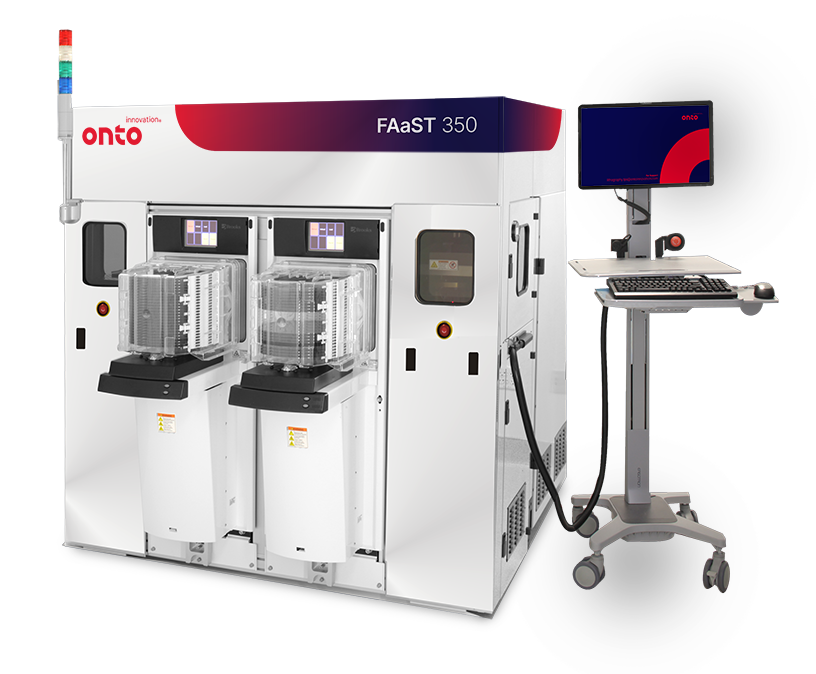
The FAaST system is a versatile, non-contact electrical metrology platform, with an option to combine micro and macro corona-Kelvin technologies together with digital surface photovoltage (SPV). It enables high-resolution dielectric and interface measurements across a wide range of dielectric materials, supporting both R&D and high volume manufacturing.
The primary application of non-contact CV metrology is monitoring dielectric properties during IC manufacturing. Unlike conventional electrical measurements, it requires no sample preparation, eliminating the need for MOS capacitor structures. This reduces metrology cost and enables fast data feedback in both R&D and manufacturing environments.
The corona-Kelvin method uses a corona discharge in air to deposit an electric charge (DQC) on the wafer surface. A vibrating Kelvin-probe then measures the resulting surface voltage (V), enabling determination of the differential capacitance (C= DQC/DV). By monitoring surface voltage in both dark and illuminated conditions, the system separates two key components: dielectric voltage (VD) and semiconductor surface potential (VSB), enabling determination of flat band voltage (VFB).
Analysis of the resulting charge-voltage data yields electrical parameters, including trap density (Dit), flat band voltage (Vfb), dielectric charge (Qtot), dielectric capacitance (CD), Equivalent Oxide Thickness (EOT), leakage current, and tunneling characteristics.
As your partner for innovative solutions, we’re always here for you.
Discover how our cutting-edge semiconductor solutions are engineered to meet your most complex challenges: delivering performance, reliability and innovation where it matters most.
"*" indicates required fields
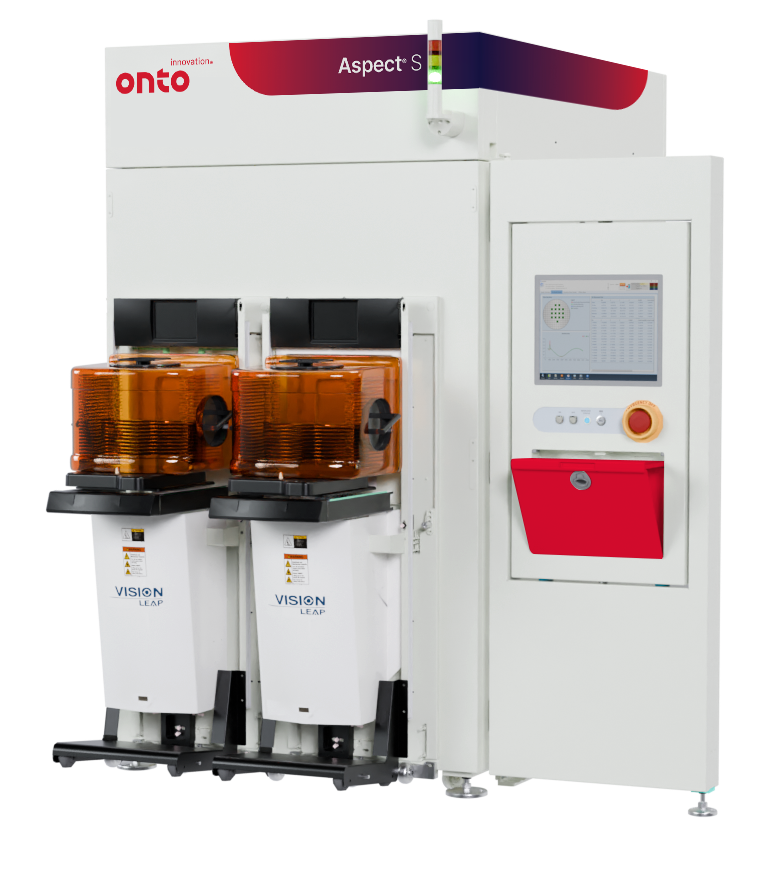
The Aspect S system is a revolutionary in-line, non-destructive model-based infrared reflectometry system that enables critical process control of high aspect ratio structures, films and epitaxial structures. It meets the needs of leading-edge customers with its high speed and process coverage.
As more high aspect ratio processes are used in multiple industry segments, there are metrology needs for monitoring of related processes, including dimensions and properties of carbon film hard masks and etched 3D structures.
The Aspect S delivers high-throughput, low COO, non-contact, non-destructive measurements of dimensions and uniformity of layers and etched structures used in integrated circuit manufacturing. The small spot size makes the tool suitable for measurements of scribe line test structures as in-line process control. The unique technology and analysis capability simplifies system calibration requirements and removes the effect of substrate variations for key layer measurements.
While the software contains advanced features for measurement recipe and analysis model creation, it has a user-friendly interface and implementation that allows the fab customers to create and manage the recipe system for Aspect S tool fleets.

Thickness map from amorphous carbon film
As your partner for innovative solutions, we’re always here for you.
Discover how our cutting-edge semiconductor solutions are engineered to meet your most complex challenges: delivering performance, reliability and innovation where it matters most.
"*" indicates required fields