
Dragonfly® G3 System
Highly configurable, automated, high speed 2D inspection and 3D metrology for inline process control in advanced packaging, specialty and front-end OQA.

Specialty devices are the unsung heroes of modern life. For many in the semiconductor industry today, the spotlight is on the SiC and GaN power devices used in automotive, green energy, fast-charge consumer electronics (CE), and high-performance computing (HPC) applications.

The Dragonfly G5 system is engineered for inline process control of leading-edge advanced packaging technologies. As the latest generation pattern inspection system in the Dragonfly series, it delivers unparalleled accuracy in detecting submicron defects and performing high-resolution 3D measurements.
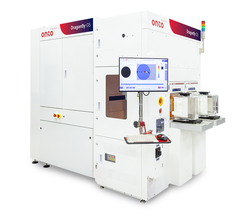
Designed to meet the demands of advanced semiconductor technologies, the Dragonfly G5 system is purpose-built to deliver high-performance, reliable inspection and metrology across complex heterogeneous integration processes. Leveraging next generation high speed line scan 2D imaging and custom-engineered objectives, the system achieves over 3X throughput improvement compared to its predecessor, with submicron sensitivity down to 150nm.
Continuing the legacy of innovation, the Dragonfly G5 system introduces a multi-angle illumination channel that significantly improves signal-to-noise ratio for faint defect detection. Combined with powerful AI-driven algorithms, it enhances both the detectability and classification of critical, yield-impacting defects–empowering fabs to maintain quality and accelerate time-to-yield.
The Dragonfly G5 system expands process control flexibility for wafer-to-wafer and die-to-wafer bonding by integrating high-speed IR imaging to detect sub-surface defects. It incorporates the latest generation of 3Di™ technology, extending bump height metrology capabilities to support next-generation microbumps essential for 3D integration. This enables additional inspection and metrology touchpoints across increasingly complex packaging architectures.


Hybrid bonding enables ultra-dense 3D memory interconnects with up to 1,000x more connections than microbumps. Achieving high yield requires stringent process control, including monitoring topography and detecting particles, cracks and voids. Measuring dishing in copper pads provides valuable insight into surface conditions. Together, these process control insights contribute to improved device reliability and performance.

As demand grows for high-performance computing (HPC) and AI-driven applications, manufacturers are turning to hybrid bonding to enable the ultra-dense 3D integration required for next-generation chip architectures. This advanced packaging technology presents significant process challenges. Surface preparation must be precisely controlled to eliminate particles, excess recess, and copper pad dishing, all of which can compromise bond quality. During pre-annealing, particle-induced gaps and wide bonding gaps can prevent proper wafer contact. Post-annealing, the formation of dielectric and metal voids introduces further risks to electrical performance and long-term reliability.

The Iris S system is a versatile platform solution for the advanced packaging and specialty market, supporting 150mm, 200mm and 300mm wafers. It provides thin and thick film, OCD and wafer bow and film stress measurements.

The IMPULSE V system helps to advance CMP processing with enhanced wavefront technology and AI-driven analytics, delivering over 2X precision improvement and faster solutions, crucial for next-gen semiconductor manufacturing demands.

The Dragonfly G5 system is engineered for inline process control of leading-edge advanced packaging technologies. As the latest generation pattern inspection system in the Dragonfly series, it delivers unparalleled accuracy in detecting submicron defects and performing high-resolution 3D measurements.

The Aspect System is a revolutionary in-line, non-destructive infrared optical critical dimension (IRCD) system measuring Z-dimension profiling of high aspect ratio structures to enable critical process control. It meets the needs of leading-edge customers with its high speed and process coverage.

As your partner for innovative solutions, we’re always here for you.
Discover how our cutting-edge semiconductor solutions are engineered to meet your most complex challenges: delivering performance, reliability and innovation where it matters most.
"*" indicates required fields
If you’ve been following the evolution of advanced packaging, you know that the industry is pushing boundaries like never before. From high-performance computing to industry-upending AI devices, the demand for smaller, faster, and more powerful chips is driving innovation at every level. One of the unsung heroes in this transformation: Glass carriers.
These carriers are becoming essential for applications involving high-bandwidth memory (HBM), 2.5D/3D integration, and chiplet architectures. During the manufacturing process, glass carriers serve as mechanical support for thin wafers and panel-level packages. Why? Glass carriers are noted for their warpage resistance, superior rigidity, and thermal stability. This combination of glass’ exceptional flatness and rigidity enables the precise placement of dies and interposers. Additionally, glass is optically transparent, which allows through-glass alignment during bonding and stacking, a critical capability for 3D integration where multiple layers must be accurately registered.
The benefits of glass carriers, however, come with several challenges, none of which should come as a surprise to anyone who has ever handled glass, whether in the fab or at home. Glass is fragile and, as such, is prone to surface defects, subsurface inclusions, and residual stress. Each of these can negatively impact die attachment quality, interconnect reliability, and die yield.
Let’s take a look at three major yield-killing culprits.
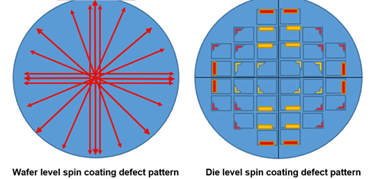
Surface defects such as particles, pits, and scratches are among the most common issues and may occur during glass carrier handling and processing, compromising the structural integrity and performance of advanced packaging assemblies (Figure 1). Particles can interfere with the bonding process, leading to poor adhesion or electrical discontinuities, while pits and scratches can propagate stress points that weaken the carrier during thermal cycling or molding.
However, subsurface inclusions and organic contamination, which are often introduced during reclaim or cleaning, pose more critical challenges. Inclusions within the glass can create localized stress concentrations, while organic residues can reduce UV transmission and cause bonding failures. These contaminants are particularly problematic in high-density interconnect environments where optical clarity and surface purity are critical.
Figure 1: Common glass carrier defects
In addition to surface and subsurface defects, residual stress represents a concern. Over time, these stress points, manifesting during thermal processing or mechanical handling, can lead to cracks or delamination, undermining the thermo-mechanical integrity of the entire package.
These potential challenges are compounded each time a glass carrier is reused in an effort to reduce overall packaging costs. Fortunately, technologies have been developed to address this obstacle. These technologies integrate AI-driven defect classification, real-time analytics, and adaptive scanning modes to maintain throughput without sacrificing accuracy, enabling manufacturers to detect surface anomalies, subsurface inclusions, and stress-induced defects with unprecedented precision.
Today’s wafer-based inspection platforms utilize laser scatterometry and imaging techniques to inspect for nanometer sized defects on a variety of opaque and transparent/semi-transparent substrates. These substrates may be suitable for either R&D or high-volume advanced IC substrate (AICS) and fan-out panel level processing (FOPLP) environments. Proprietary inspection technology with multiple detection channels and advanced signal processing algorithms is applied to achieve accuracy and reliability in glass carrier inspection.
Figure 2: Results of top (blue) and bottom (red) defect mapping.
With each channel optimized to capture unique scattering and reflection signatures, the technology differentiates between surface and subsurface defects, as well as stress-related anomalies, with remarkable accuracy. Surface particles, scratches, pits, bumps, surface contamination, film or bulk wafer stress, voids/inclusions can be detected, measured, characterized, and imaged. One of the most significant capabilities of this technology is the ability to conduct simultaneous top, bottom, and internal defect mapping, a critical need for transparent and semi-transparent substrates where defects can occur across multiple planes (Figure 2).
Beyond defect detection, Angstrom-level film thickness measurement provides precise control over surface coatings and residual layers. This capability is particularly valuable in the glass reclaim process where even minor variations in film thickness can impact UV transmission and bonding performance. By enabling accurate defect detection and grading, only glass carriers meeting stringent quality standards are returned to production.
By introducing technologies that mitigate risks by providing comprehensive defect mapping and stress analysis, manufacturers are able to maintain the mechanical and thermal integrity required for next-generation devices. This capability is especially valuable in markets such as AI devices, high-performance computing, and automotive electronics where reliability is non-negotiable. With this combination of advanced optical technology and robust algorithmic analysis, manufacturers can successfully achieve higher yields, lower costs, and greater confidence in their packaging processes.
As packaging complexity grows and the use of glass carriers increases, inspection systems that combine multi-depth defect mapping and stress analysis will become indispensable for ensuring yield and reliability in AI and HPC devices. With the explosive growth in AI-driven data centers and advanced packaging architectures, manufacturers need solutions that combine accuracy, speed, and cost efficiency. The laser-based wafer inspection technology discussed in this blog meets several glass carrier challenges head-on while enabling advanced packaging houses to maintain defect-free glass carriers in support of next-generation advanced packaging.
The future of glass carriers is clear: with the right technologies at the ready, manufacturers have the tools and the means to meet the growing needs of the AI and HPC markets.
Jason Lin is Director of Product Marketing at Onto Innovation.
We’d love to connect with you.
Looking to learn more about our innovative solutions and capabilities? Our team of experts is ready to assist you. Reach out today and let’s starts a conversation about how we can help you achieve your goals.
"*" indicates required fields
The FAaST system is a versatile, non-contact electrical metrology platform, with an option to combine micro and macro corona-Kelvin technologies together with digital surface photovoltage (SPV). It enables high-resolution dielectric and interface measurements across a wide range of dielectric materials, supporting both R&D and high volume manufacturing.
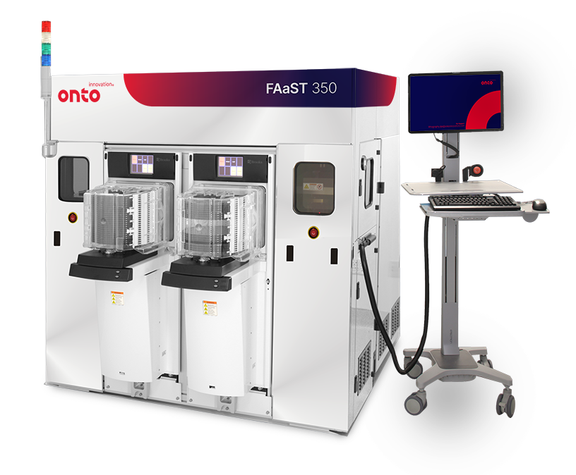
The primary application of non-contact CV metrology is monitoring dielectric properties during IC manufacturing. Unlike conventional electrical measurements, it requires no sample preparation, eliminating the need for MOS capacitor structures. This reduces metrology cost and enables fast data feedback in both R&D and manufacturing environments.
The corona-Kelvin method uses a corona discharge in air to deposit an electric charge (DQC) on the wafer surface. A vibrating Kelvin-probe then measures the resulting surface voltage (V), enabling determination of the differential capacitance (C= DQC/DV). By monitoring surface voltage in both dark and illuminated conditions, the system separates two key components: dielectric voltage (VD) and semiconductor surface potential (VSB), enabling determination of flat band voltage (VFB).
Analysis of the resulting charge-voltage data yields electrical parameters, including trap density (Dit), flat band voltage (Vfb), dielectric charge (Qtot), dielectric capacitance (CD), Equivalent Oxide Thickness (EOT), leakage current, and tunneling characteristics.
As your partner for innovative solutions, we’re always here for you.
Discover how our cutting-edge semiconductor solutions are engineered to meet your most complex challenges: delivering performance, reliability and innovation where it matters most.
"*" indicates required fields
The PrimaScan wafer defect inspection system delivers a flexible, high sensitivity solution at the lowest cost of ownership per pass.
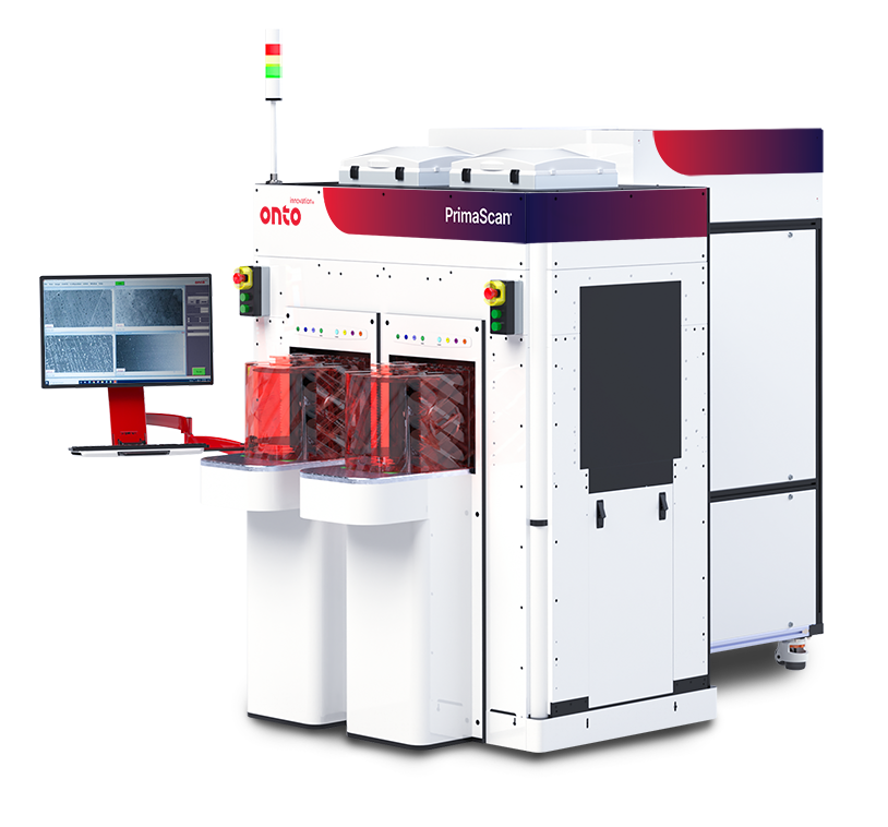
The PrimaScan system utilizes laser scatterometry and imaging techniques leveraging proprietary optics and sensing technologies for reliable inspection of nanometer sized defects on a variety of opaque and transparent/semi-transparent substrates suitable for either R&D or high-volume manufacturing environments. With multiple detection channels, the system can detect, measure, characterize and image surface particles, scratches, pits, bumps, surface contamination, film or bulk wafer stress, voids/inclusions, including chips and cracks at the wafer edge.
The PrimaScan system addresses challenges in both incoming wafer quality control and in inline process monitoring. Capable of handling multiple substrate materials, it uniquely addresses inline process defect and contamination monitoring in wafer-based production environments.
Designed with versatility in mind the PrimaScan system can handle a variety of wafer sizes and substrate types


As your partner for innovative solutions, we’re always here for you.
Discover how our cutting-edge semiconductor solutions are engineered to meet your most complex challenges: delivering performance, reliability and innovation where it matters most.
"*" indicates required fields
The NSX 330 system offers advanced macro inspection for a wide range of defect sizes at high throughput, with optional 3D metrology integration.
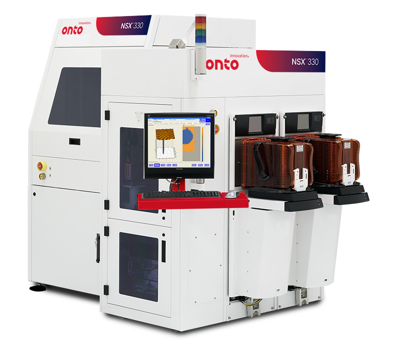
The NSX 330 system features robust platform technology with high-acceleration staging, high-speed multi-processor computing and flexible software. With over 1,000 installation worldwide, the NSX 330 System offers 2D inspection and metrology at high throughput and a broad portfolio of 3D sensors supporting critical advanced packaging applications. These include wafer-level metrology for micro bumps, RDL, kerf, overlay, and through silicon via (TSV) in a single wafer load.
Accommodating wafers from 100mm to 330mm, the system features a versatile objective turret, programmable light tower, and multiple dark field illumination modes. Additional features include resolution flexibility, unique handling solutions, and comprehensive software for recipe sharing and offline analysis. The NSX 330 system, with optional edge and backside inspection via the EB40 module, provides a comprehensive all-surface inspection solution packaging technology challenges.
As your partner for innovative solutions, we’re always here for you.
Discover how our cutting-edge semiconductor solutions are engineered to meet your most complex challenges: delivering performance, reliability and innovation where it matters most.
"*" indicates required fields
The F30 system is designed to blur the lines between dark field micro inspection and traditional macro inspection, providing automated defect inspection for front-end and outgoing quality (OQA) applications.
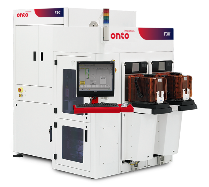
The F30 automated defect inspection system combines high resolution and throughput to drive fab yield and productivity. A five-objective turret enables resolution-throughput flexibility, while its multi-channel illumination including brightfield, darkfield, high-angle ring light, and IR-Review addresses the requirements for today’s multi-process inspection applications. Equipped with an advanced productivity suite (waferless recipe creation, simultaneous FOUP, recipe server and tool matching), the F30 System redefines inspection cost of ownership expectations. The system can handle 100mm – 300mm wafers can be paired with the edge and backside module (EB40) to provide an all-surface inspection solution.
As your partner for innovative solutions, we’re always here for you.
Discover how our cutting-edge semiconductor solutions are engineered to meet your most complex challenges: delivering performance, reliability and innovation where it matters most.
"*" indicates required fields