Atlas® III+ System

The Atlas III+ system provides dependable OCD and thin film metrology for established technologies, with flexible performance across a wide range of process layers and device types.

Atlas® III+ System

Product Overview

The Atlas III+ system is a widely adopted inline OCD metrology system, known for its robust and reliable solutions across all OCD and film layers from FEOL to BEOL. With its information-rich optical architecture, powerful OCD and machine learning analysis engine, the Atlas III+ system excels in advanced logic, 3D NAND and DRAM device processes. Extending metrology performance to sub-angstrom precision and accuracy levels, this system enables advanced process control across a broad range of applications in high volume manufacturing. The Atlas III+ system incorporates a proprietary spectroscopic reflectometry and spectroscopic ellipsometry solution, and when combined with Onto Innovation’s Ai Diffract™ OCD analysis software, it enables process control of every critical manufacturing unit operation. Users can gain insights into complex structure profiles across etch, clean, deposition and CMP steps.

Applications

  • 3D-NAND
  • DRAM: Logic and Foundry
  • Specialty: CIS, AR/VR, Power & RF etc.
Related Products
View all
Atlas-G6-NEWBRAND-featured-720×400

Atlas® G6 System

Leading edge OCD and thin film metrology for next-generation AI applications and beyond.
View Product
atlasv_feat

Atlas® V System

High performance OCD and thin film metrology for advanced GAA and memory devices.
View Product
impulse v_feat

IMPULSE® V System

Advanced high throughput integrated metrology system with AI-driven machine learning option. The system offers maximum sensitivity and accuracy to CMP process excursions and enables process engineers to establish APC control with high-accuracy feedback.
View Product
impulse+_feat

IMPULSE®+ System

Integrated metrology system offering maximum sensitivity and accuracy to CMP process excursions and enabling process engineers to establish APC control with high-accuracy feedback.
View Product
aspect_feat

Aspect® System

Advanced infrared optical critical dimension (IRCD) metrology system for high aspect ratio structures in 3D NAND, 2D & 3D DRAM, CIS and power devices.
View Product
ocdsolutions_aidiffract_feat

OCD Solutions

A suite of OCD modeling software and computing hardware offering comprehensive capabilities for inline metrology, offline recipe creation and fleet management.
View Product
Related Insights & Resources
View all
GAA

Optical Critical Dimension Metrology for Semiconductor Manufacturing

Learn more

Do you have an Atlas III+ system question? Let’s talk!

As your partner for innovative solutions, we’re always here for you.

Discover how our cutting-edge semiconductor solutions are engineered to meet your most complex challenges: delivering performance, reliability and innovation where it matters most.

Let’s Talk

"*" indicates required fields

This field is for validation purposes and should be left unchanged.

Atlas® V System

The Atlas V system is an OCD and thin film metrology tool for high volume manufacturing, enabling FinFET & Gate-All-Around (GAA) logic, DRAM, and 3D NAND device process control.

Atlas® V System

Product Overview

The Atlas V system combines state of the art optical design with an innovative Ai Diffract modeling engine, providing OCD and thin film metrology solutions for measuring complex 3D device structures. The dual channel optical architecture consists of a DUV 4×4 Mueller Matrix (MM) SE and a DUV polarized normal incident reflectometer (NIOCD). Together, they provide rich information for OCD analysis at high precision and high throughput. The Atlas V system is designed to measure the most critical and challenging process steps that include buried features, not visible by CD-SEM and other techniques.

With unique capabilities, such as measuring individual nanowire dimension in a GAA logic device, the Atlas V system is an enabling technology for leading edge device process control.

Applications

  • OCD for litho, etch, CVD & CMP process in all device segments
  • Local variation
  • Asymmetry and tilt
  • Common and critical films
  • Stress & wafer warpage
Related Products
View all
Atlas-G6-NEWBRAND-featured-720×400

Atlas® G6 System

Leading edge OCD and thin film metrology for next-generation AI applications and beyond.
View Product
atlasiii_feat

Atlas® III+ System

Versatile OCD and thin film metrology for mature and mainstream nodes.
View Product
impulse v_feat

IMPULSE® V System

Advanced high throughput integrated metrology system with AI-driven machine learning option. The system offers maximum sensitivity and accuracy to CMP process excursions and enables process engineers to establish APC control with high-accuracy feedback.
View Product
impulse+_feat

IMPULSE®+ System

Integrated metrology system offering maximum sensitivity and accuracy to CMP process excursions and enabling process engineers to establish APC control with high-accuracy feedback.
View Product
aspect_feat

Aspect® System

Advanced infrared optical critical dimension (IRCD) metrology system for high aspect ratio structures in 3D NAND, 2D & 3D DRAM, CIS and power devices.
View Product
ocdsolutions_aidiffract_feat

OCD Solutions

A suite of OCD modeling software and computing hardware offering comprehensive capabilities for inline metrology, offline recipe creation and fleet management.
View Product
Related Insights & Resources
View all
impulse-1-duo

Enhancing CMP Process Control with Intelligent Line Monitoring & Integrated Metrology

Learn more
high-profile-dram

Non-destructive Metrology Techniques for Measuring Hole Profile in DRAM Storage Node

Learn more
GAA

Optical Critical Dimension Metrology for Semiconductor Manufacturing

Learn more
fig-1_200720_065724

Metrology Solutions for Gate-All-Around Transistors in High Volume Manufacturing

Learn more

Do you have an Atlas V system question? Let’s talk!

As your partner for innovative solutions, we’re always here for you.

Discover how our cutting-edge semiconductor solutions are engineered to meet your most complex challenges: delivering performance, reliability and innovation where it matters most.

Let’s Talk

"*" indicates required fields

This field is for validation purposes and should be left unchanged.

Aspect® System

The Aspect System is a revolutionary in-line, non-destructive infrared optical critical dimension (IRCD) system measuring Z-dimension profiling of high aspect ratio structures to enable critical process control. It meets the needs of leading-edge customers with its high speed and process coverage.

Aspect® System

Product Overview

As the semiconductor industry relentlessly pursues density and power scaling, more and more high aspect ratio (HAR) processes are used across multiple device segments, especially in advanced memory such as 3D NAND and 3D DRAM. The Aspect metrology system was designed with these ongoing architectures and scaling strategies in mind. Aspect metrology has demonstrated superior performance across multiple customer devices through a unique proprietary IRCD system that provides full profiling capability to enable critical process control, with the speed and process coverage that customers require.

The Aspect system is powered by a software analysis engine, Ai Diffract™, that provides up to 90% faster time to solution which extends the industry leading NanoDiffract® software by leveraging extensive machine learning capabilities along with high fidelity modeling. The result is a simultaneous improvement in metrology performance along with a significant time to solution reduction.

Applications

  • Etch, cleans, and deposition for 3D NAND
  • Etch, cleans, and deposition for 2D and 3D DRAM
  • Deep trench etch and doping for CIS
  • Deep Trench etch in Power Devices
  • On-device materials characterization for EPI process
Related Products
View all
atlasv_feat

Atlas® V System

High performance OCD and thin film metrology for advanced GAA and memory devices.
View Product
atlasiii_feat

Atlas® III+ System

Versatile OCD and thin film metrology for mature and mainstream nodes.
View Product
element s_feat

Element™ S System

Transmission and reflection combined FTIR Measurement for wafer, specialty devices, supporting 100-200mm wafer sizes.
View Product
elementg2_feat

Element™ G2 System

Transmission and reflection combined FTIR measurement for advanced epi thickness, film composition control and advanced IR modeling.
View Product
MBIR System _feat2

MBIR System 

Advanced model-based infrared reflectometry (MBIR) metrology system for in-line monitoring of 3D structures used in V-NAND, CIS and power devices, as well as carbon hardmasks, dielectric compositions and epitaxial layer stacks.
View Product
Related Insights & Resources
View all
Deep-trench

Non-destructive Measurement of Bottom Width in Deep Trench Isolation Structures Using IRCD Metrology

Learn more
new-technique

Measuring the Critical W-recess in 3D NAND

Learn more
IRCD_220208_132903

Critical Moves: Advanced Logic Devices And CIS Benefit From Applications Using IRCD Metrology

Learn more
aspect-social

Mid-Infrared Optical Metrology for High Aspect Ratio Holes in 3D NAND Memory Manufacturing

Learn more
3D-Nand2

Untangling 3D NAND: Tilt, Registration, and Misalignment

Learn more

Do you have an Aspect system question? Let’s talk!

As your partner for innovative solutions, we’re always here for you.

Discover how our cutting-edge semiconductor solutions are engineered to meet your most complex challenges: delivering performance, reliability and innovation where it matters most.

Let’s Talk

"*" indicates required fields

This field is for validation purposes and should be left unchanged.

PrecisionWoRx® VX4 System

The PrecisionWoRx VX4 System is designed to provide accurate and repeatable performance through enhanced testing of the latest probe card technologies with tighter pitches, smaller pads and higher pin counts.

PrecisionWoRx® VX4 System

Product Overview

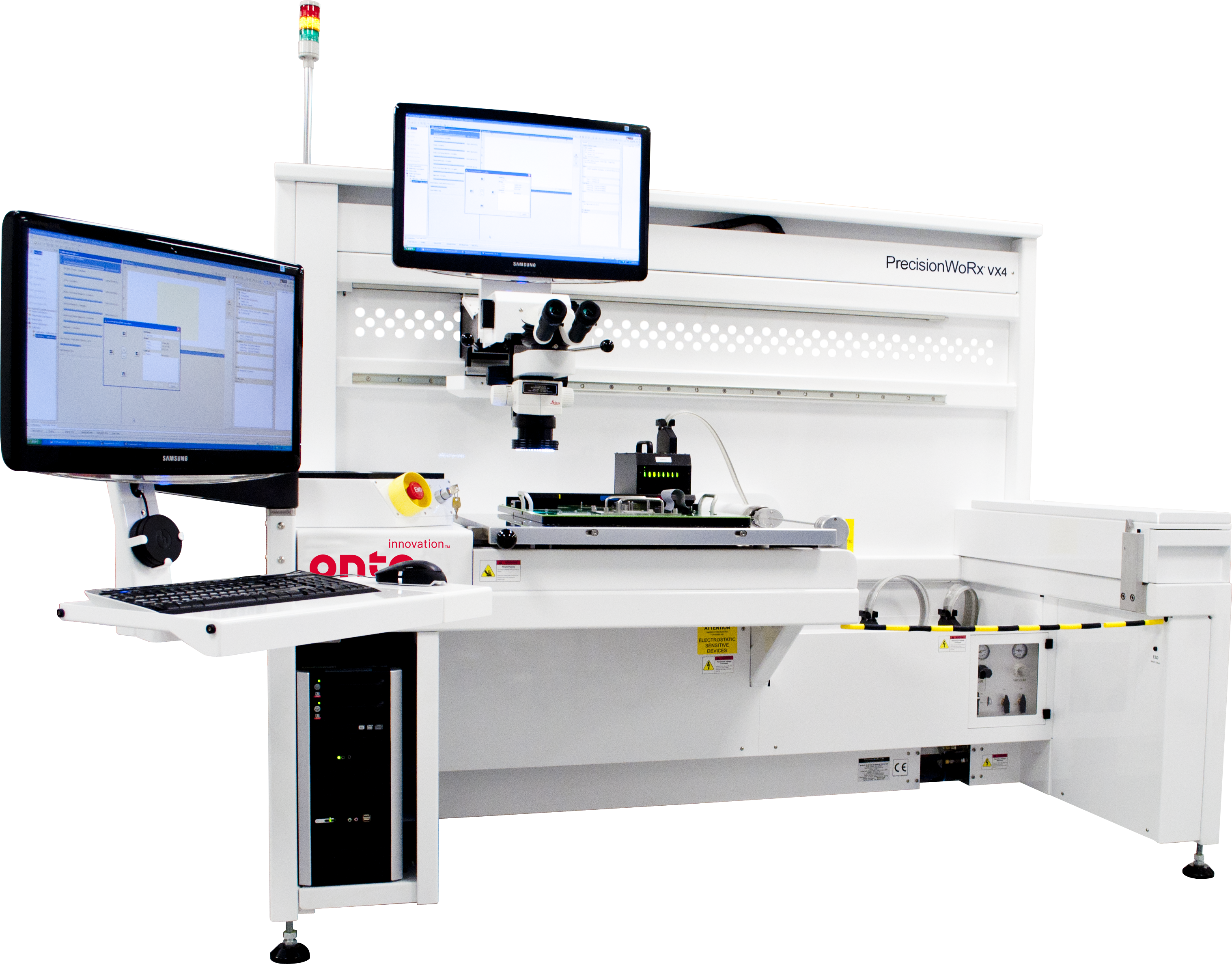
The PrecisionWoRx VX4 System gives test facilities and probe card manufacturers the ability to confidently test tighter pitches and smaller probe tips. The system can be configured to meet specific requirements for a variety of probe card technologies. For processes using cards with very small probe tips, the system’s high-resolution optics deliver a detailed field-of-view for high accuracy and repeatability. Proprietary image-processing recipes control over 30 imaging parameters for enhanced testing of most probe tip geometries in use today.

The PrecisionWoRx VX4 System improves overall cost of ownership with faster test times for common tests, including leakage, planarity, alignment, contact resistance, probe force and wire checker. Its sophisticated electrical discharge management capability maintains 1-volt continuity to the probe during electrical testing. Productivity-enhanced routines for automated testing of failed probes and a wide variety of checkplates suit an extensive range of process and technology requirements. The system provides support for the most complex probe card technologies.

Applications

  • Various probe tips from 5 µm up to 250 µm diameter
  • Z force up to 200 KG
  • Pin counts >100,000 probes
  • Direct dock probe card capabilities
  • Probe card relay and solid-state switching
  • Membrane probe cards
Related Products
View all
primascan_feat

PrimaScan™ System

All-surface defect and contamination inspection for unpatterned wafer and blanket films, with imaging capability for opaque, transparent and semi-transparent wafers, reticles and piece parts.
View Product
primascan r&d_feat

PrimaScan™ R&D System

All-surface defect and contamination inspection for unpatterned wafer and blanket films, with imaging capability for opaque, transparent and semi-transparent wafers, reticles and piece parts.
View Product
dragonfly g3_feat

Dragonfly® G3 System

Automated high speed sub-micron 2D inspection and 3D inspection/metrology for inline process control of pattern defects in next generation technologies for advanced packaging, specialty and OQA.
View Product
novudedge_feat

NovusEdge® G2 System

Unpatterned edge, notch and backside inspection.
View Product
celeroPL_feat

Celero™ PL System

Subsurface defect and crystalline defect inspection and classification in bulk and epitaxial III-V materials for application in power semiconductors.
View Product

Do you have a PrecisionWoRx VX4 system question? Let’s talk!

As your partner for innovative solutions, we’re always here for you.

Discover how our cutting-edge semiconductor solutions are engineered to meet your most complex challenges: delivering performance, reliability and innovation where it matters most.

Let’s Talk

"*" indicates required fields

This field is for validation purposes and should be left unchanged.

F30™ System

The F30 system is designed to blur the lines between dark field micro inspection and traditional macro inspection, providing automated defect inspection for front-end and outgoing quality (OQA) applications.

F30™ System

Product Overview

The F30 automated defect inspection system combines high resolution and throughput to drive fab yield and productivity. A five-objective turret enables resolution-throughput flexibility, while its multi-channel illumination including brightfield, darkfield, high-angle ring light, and IR-Review addresses the requirements for today’s multi-process inspection applications. Equipped with an advanced productivity suite (waferless recipe creation, simultaneous FOUP, recipe server and tool matching), the F30 System redefines inspection cost of ownership expectations. The system can handle 100mm – 300mm wafers can be paired with the edge and backside module (EB40) to provide an all-surface inspection solution.

Applications

  • After develop inspection (ADI)
  • Post CMP inspection
  • After etch inspection
  • Fab Outgoing QA
Related Products
View all
discoverdefect_feat

Discover® Defect Software

Integrated defect management system that works seamlessly with Onto tools and your entire enterprise, bringing data together for greater visibility and cleaner operation.
View Product
trueadc_feat

TrueADC® Software

Automated defect classification software with deep learning, real defect modeling and seamless integration with Onto AOI tools.
View Product

Do you have a F30 system question? Let’s talk!

As your partner for innovative solutions, we’re always here for you.

Discover how our cutting-edge semiconductor solutions are engineered to meet your most complex challenges: delivering performance, reliability and innovation where it matters most.

Let’s Talk

"*" indicates required fields

This field is for validation purposes and should be left unchanged.

Celero™ PL System

The Celero PL system is designed for subsurface defect inspection and classification for silicon carbide (SiC) and gallium nitride (GaN) based wafers and compound semiconductor materials.

Celero™ PL System

Product Overview

The Celero PL system utilizes a laser-based phase detection and imaging capability that leverages custom optics and image processing algorithms to enable best in class throughput and sensitivity for silicon carbide and gallium nitride-based materials on 100mm to 300mm wafer sizes. Leveraging multiple light sources and sensor channels, the system can detect, measure and image a broad variety of subsurface crystalline defects, associated with bulk wafers and epitaxial layers, surface particles, scratches, pits, surface contamination, stains, point or bulk wafer stress, voids/inclusions, including chips and cracks at the edge of the wafer.

Applications

  • Frontside / backside / edge / subsurface defectivity and contamination
  • Crystalline defectivity in III-V substrates and epitaxial layers
  • Thick wafer / seed wafer surface and sub-surface defectivity
  • Substrate-to-epitaxial layer defect mapping (sub-defect mapping)
  • Wafer based microLED / VCSEL / EE laser materials
Related Products
View all
primascan_feat

PrimaScan™ System

All-surface defect and contamination inspection for unpatterned wafer and blanket films, with imaging capability for opaque, transparent and semi-transparent wafers, reticles and piece parts.
View Product
primascan r&d_feat

PrimaScan™ R&D System

All-surface defect and contamination inspection for unpatterned wafer and blanket films, with imaging capability for opaque, transparent and semi-transparent wafers, reticles and piece parts.
View Product

Do you have a Celero PL system question? Let’s talk!

As your partner for innovative solutions, we’re always here for you.

Discover how our cutting-edge semiconductor solutions are engineered to meet your most complex challenges: delivering performance, reliability and innovation where it matters most.

Let’s Talk

"*" indicates required fields

This field is for validation purposes and should be left unchanged.