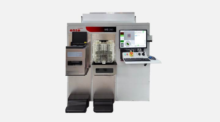
IVS 280 System
Overlay, CD and height metrology for 100mm-200mm wafers in the compound semiconductor, power devices, RF, MEMS and LED markets.

If you’ve been following the evolution of advanced packaging, you know that the industry is pushing boundaries like never before. From high-performance computing to industry-upending AI devices, the demand for smaller, faster, and more powerful chips is driving innovation at every level.

The IVS 380 System delivers overlay, CD and z-height metrology for advanced packaging, power, compound semi and MEMS, offering world class performance and flexibility to accommodate substrates of different sizes and thickness without hardware changes.
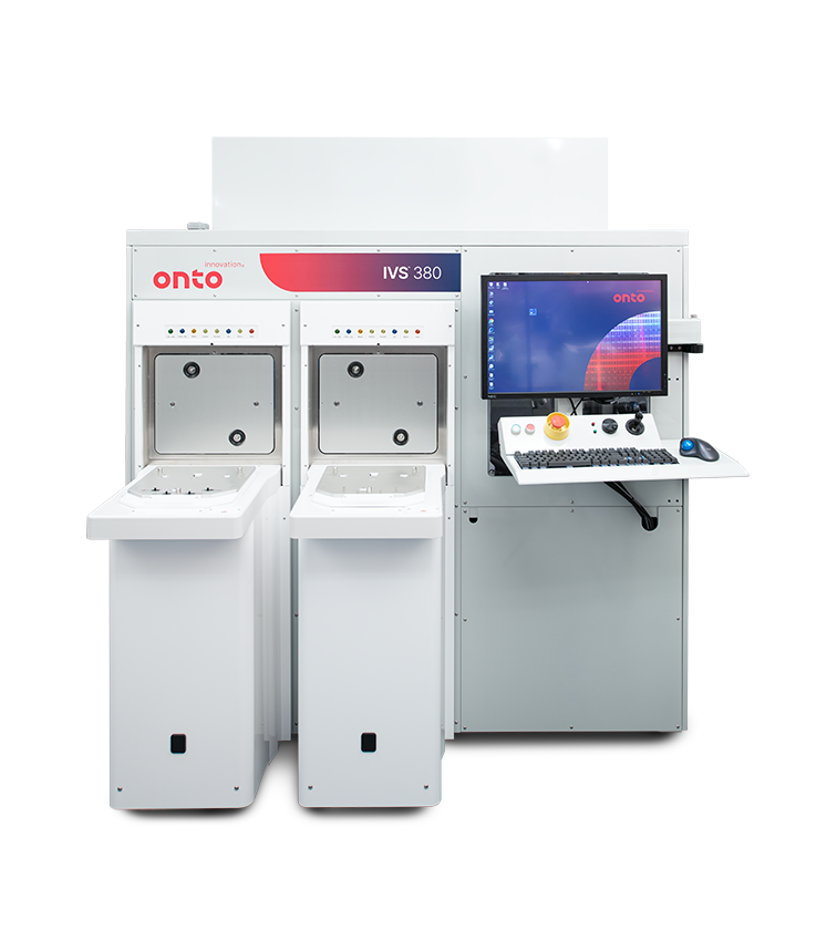
The IVS 380 is an optical overlay, CD & z-height metrology system designed for high volume manufacturing, with SMIF (200mm substrate) or FOUP (300mm substrate) load ports compatibility. It handles various substrates for advanced packaging, including Si, glass and CCL, and accommodates sizes of 200mm and 300mm.
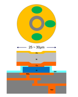
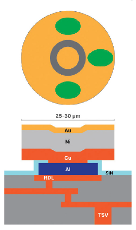
Building on the IVS family’s 40 years of experience in CMOS, MEMS and compound semiconductor applications, the IVS 380 system possesses the versatility to tackle overlay, CD and z-height measurements for diverse substrates and layers. It measures critical dimensions in the xy plane and the vertical z-heights of features like RDL metal lines, posts and bumps. The optics enable focus on mostly transparent materials such as photoresists and rough surfaces such as electroplated copper.
Enter your information below and we’ll send you a unique passcode to view our IVS 3D Demo.

As your partner for innovative solutions, we’re always here for you.
Discover how our cutting-edge semiconductor solutions are engineered to meet your most complex challenges: delivering performance, reliability and innovation where it matters most.
"*" indicates required fields
The Iris G2 system is an advanced optical metrology tool for both common and critical thin films for advanced node, mature and specialty devices, enabling manufacturers to increase transistor speed, reduce power consumption and improve reliability.
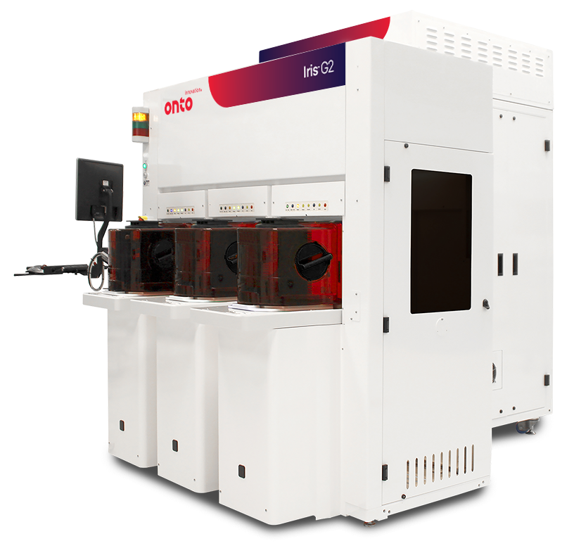
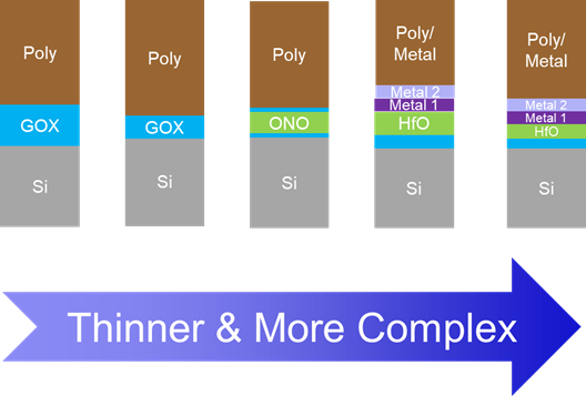
As semiconductor device technologies become increasingly complex, requiring thinner and more uniform films, the need for a stable, all-in-one thin film metrology solution becomes a necessity. By controlling the quality and effective thickness of gate films, the Iris G2 system supports critical device scaling and performance improvements.
For ultra-thin multilayer films measuring 10Å to 50Å, the Iris G2 system features deep ultraviolet (DUV) spectroscopic ellipsometry (SE) for common films and coupled proprietary laser ellipsometry technologies for critical films, providing customers with the flexibility to optimize cost of ownership, better stability, and ease of operation in a versatile tool for specialty, mature and advanced logic and memory processes.
Additionally, a single platform simplifies fleet management and fab operations while reducing overall capital investment.
Enhance CMP process control with a connected metrology approach that feeds forward data from standalone OCD or films metrology to integrated metrology, connected through AI-driven analytical software. This approach, powered by advanced modeling and analysis tools, can deliver high-precision, high-throughput results—minimizing or eliminating the need for and cost of new TEM data and enabling accelerated time to solution, faster excursion detection, reduced cost and improved Cpk.

As semiconductor manufacturers push the boundaries of performance and functionality—driven by high-performance computing and AI applications—chemical mechanical planarization (CMP) processes increase in intensity complexity. New logic transistor designs, 3D NAND stacking, and DRAM integration introduce more CMP layers and tighter process windows.

The IMPULSE V system helps to advance CMP processing with enhanced wavefront technology and AI-driven analytics, delivering over 2X precision improvement and faster solutions, crucial for next-gen semiconductor manufacturing demands.

The IMPULSE+ system is designed to deliver film measurement, fidelity and productivity in the CMP process module. Available as an integrated or standalone platform, it offers high sensitivity and accuracy.

The Atlas V system is an OCD and thin film metrology tool for high volume manufacturing, enabling FinFET & Gate-All-Around (GAA) logic, DRAM, and 3D NAND device process control.

The Atlas III+ system provides dependable OCD and thin film metrology for established technologies, with flexible performance across a wide range of process layers and device types.

The Iris S system is a versatile platform solution for the advanced packaging and specialty market, supporting 150mm, 200mm and 300mm wafers. It provides thin and thick film, OCD and wafer bow and film stress measurements.
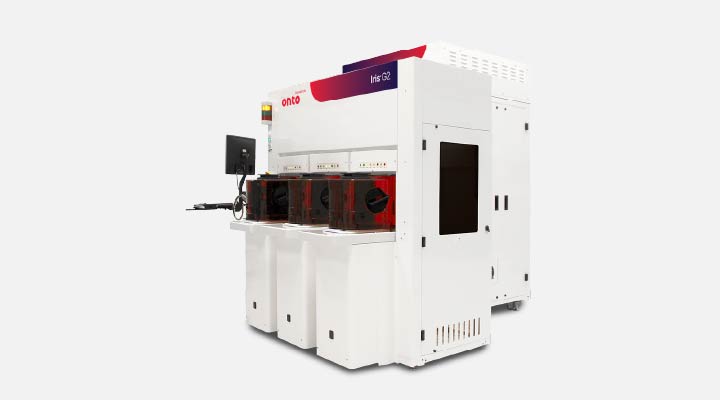
The Iris G2 system is an advanced optical metrology tool for both common and critical thin films for advanced node, mature and specialty devices, enabling manufacturers to increase transistor speed, reduce power consumption and improve reliability.

A suite of OCD modeling software and computing hardware that enables the full capability and connectivity across all Onto OCD and thin film metrology systems, including Atlas, Aspect, Iris and IMPULSE systems.
As your partner for innovative solutions, we’re always here for you.
Discover how our cutting-edge semiconductor solutions are engineered to meet your most complex challenges: delivering performance, reliability and innovation where it matters most.
"*" indicates required fields
The IMPULSE+ system is designed to deliver film measurement, fidelity and productivity in the CMP process module. Available as an integrated or standalone platform, it offers high sensitivity and accuracy.
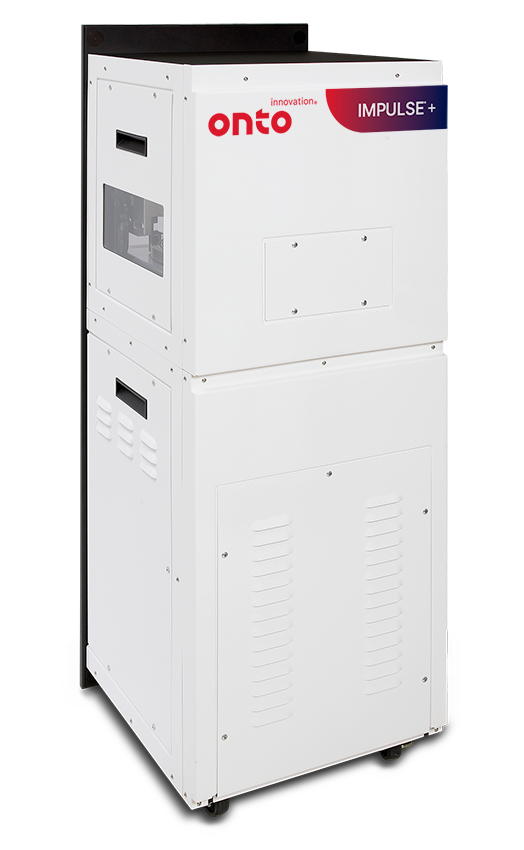
An integrated metrology standard, the IMPULSE+ system offers high sensitivity and accuracy to CMP process excursions and enables device makers to establish APC control with high-accuracy feedback. The IMPULSE+ system works in conjunction with the Atlas® platform, facilitating cross-module process optimization and comprehensive fab-wide process control.
Based on a common optical design derived from our stand-alone Atlas® platform, the IMPULSE+ system shares superior deep ultraviolet (DUV) optics. This unique ecosystem can be leveraged to improve signal to noise ratio by applying spectra feedforward from the Atlas platform, further enhanced by AI-driven machine analytics. This combination affords CMP process engineers a potent arsenal of capability to manage excursions and drive process improvement (Cpk.).
The IMPULSE+ system is widely adopted across key steps in DRAM, 3D-NAND, CMOS image sensor and foundry/logic device manufacturing. challenging to measure.
Enhance CMP process control with a connected metrology approach that feeds forward data from standalone OCD or films metrology to integrated metrology, connected through AI-driven analytical software. This approach, powered by advanced modeling and analysis tools, can deliver high-precision, high-throughput results—minimizing or eliminating the need for and cost of new TEM data and enabling accelerated time to solution, faster excursion detection, reduced cost and improved Cpk.
As semiconductor manufacturers push the boundaries of performance and functionality—driven by high-performance computing and AI applications—chemical mechanical planarization (CMP) processes increase in intensity complexity. New logic transistor designs, 3D NAND stacking, and DRAM integration introduce more CMP layers and tighter process windows.
The IMPULSE V system helps to advance CMP processing with enhanced wavefront technology and AI-driven analytics, delivering over 2X precision improvement and faster solutions, crucial for next-gen semiconductor manufacturing demands.
The IMPULSE+ system is designed to deliver film measurement, fidelity and productivity in the CMP process module. Available as an integrated or standalone platform, it offers high sensitivity and accuracy.
The Atlas V system is an OCD and thin film metrology tool for high volume manufacturing, enabling FinFET & Gate-All-Around (GAA) logic, DRAM, and 3D NAND device process control.
The Atlas III+ system provides dependable OCD and thin film metrology for established technologies, with flexible performance across a wide range of process layers and device types.
The Iris S system is a versatile platform solution for the advanced packaging and specialty market, supporting 150mm, 200mm and 300mm wafers. It provides thin and thick film, OCD and wafer bow and film stress measurements.
The Iris G2 system is an advanced optical metrology tool for both common and critical thin films for advanced node, mature and specialty devices, enabling manufacturers to increase transistor speed, reduce power consumption and improve reliability.
A suite of OCD modeling software and computing hardware that enables the full capability and connectivity across all Onto OCD and thin film metrology systems, including Atlas, Aspect, Iris and IMPULSE systems.
As your partner for innovative solutions, we’re always here for you.
Discover how our cutting-edge semiconductor solutions are engineered to meet your most complex challenges: delivering performance, reliability and innovation where it matters most.
"*" indicates required fields
The IMPULSE V system helps to advance CMP processing with enhanced wavefront technology and AI-driven analytics, delivering over 2X precision improvement and faster solutions, crucial for next-gen semiconductor manufacturing demands.
As wafer uniformity requirements tighten and vertical scaling increases, the need for CMP processing grows across market segments. Logic introduces new transistor designs and materials, DRAM incorporates new materials and process steps to planarize, and 3D NAND adds more decks, stacks and tiers.
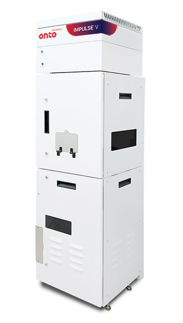
The IMPULSE V system, available as an integrated or standalone platform, enhances film measurement fidelity and productivity for the CMP process module. With deep ultraviolet (DUV) optics and AI-driven machine analytics derived from our Atlas® platform, it works in conjunction with the Atlas® platform to provide CMP process engineers the capability to manage excursions and drive process improvement (Cpk.).
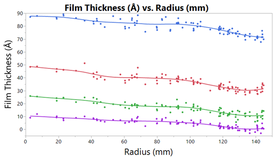
Advanced wavefront technology suppresses previous layer noise in complex structures. It provides feedback to improve long term repeatability. Designed for higher sampling, in-die/on-device and wafer edge measurements, the system offers improved reliability, higher throughput and over 2X precision improvement compared to the previous generation. Onboard AI-driven machine learning uses a signal-to-noise ratio for faster time-to-solution, addressing layers that were previously challenging to measure.
Enhance CMP process control with a connected metrology approach that feeds forward data from standalone OCD or films metrology to integrated metrology, connected through AI-driven analytical software. This approach, powered by advanced modeling and analysis tools, can deliver high-precision, high-throughput results—minimizing or eliminating the need for and cost of new TEM data and enabling accelerated time to solution, faster excursion detection, reduced cost and improved Cpk.
As semiconductor manufacturers push the boundaries of performance and functionality—driven by high-performance computing and AI applications—chemical mechanical planarization (CMP) processes increase in intensity complexity. New logic transistor designs, 3D NAND stacking, and DRAM integration introduce more CMP layers and tighter process windows.
The IMPULSE V system helps to advance CMP processing with enhanced wavefront technology and AI-driven analytics, delivering over 2X precision improvement and faster solutions, crucial for next-gen semiconductor manufacturing demands.
The IMPULSE+ system is designed to deliver film measurement, fidelity and productivity in the CMP process module. Available as an integrated or standalone platform, it offers high sensitivity and accuracy.
The Atlas V system is an OCD and thin film metrology tool for high volume manufacturing, enabling FinFET & Gate-All-Around (GAA) logic, DRAM, and 3D NAND device process control.
The Atlas III+ system provides dependable OCD and thin film metrology for established technologies, with flexible performance across a wide range of process layers and device types.
The Iris S system is a versatile platform solution for the advanced packaging and specialty market, supporting 150mm, 200mm and 300mm wafers. It provides thin and thick film, OCD and wafer bow and film stress measurements.
The Iris G2 system is an advanced optical metrology tool for both common and critical thin films for advanced node, mature and specialty devices, enabling manufacturers to increase transistor speed, reduce power consumption and improve reliability.
A suite of OCD modeling software and computing hardware that enables the full capability and connectivity across all Onto OCD and thin film metrology systems, including Atlas, Aspect, Iris and IMPULSE systems.
Hybrid bonding enables ultra-dense 3D memory interconnects with up to 1,000x more connections than microbumps. Achieving high yield requires stringent process control, including monitoring topography and detecting particles, cracks and voids. Measuring dishing in copper pads provides valuable insight into surface conditions. Together, these process control insights contribute to improved device reliability and performance.

As demand grows for high-performance computing (HPC) and AI-driven applications, manufacturers are turning to hybrid bonding to enable the ultra-dense 3D integration required for next-generation chip architectures. This advanced packaging technology presents significant process challenges. Surface preparation must be precisely controlled to eliminate particles, excess recess, and copper pad dishing, all of which can compromise bond quality. During pre-annealing, particle-induced gaps and wide bonding gaps can prevent proper wafer contact. Post-annealing, the formation of dielectric and metal voids introduces further risks to electrical performance and long-term reliability.
The Iris S system is a versatile platform solution for the advanced packaging and specialty market, supporting 150mm, 200mm and 300mm wafers. It provides thin and thick film, OCD and wafer bow and film stress measurements.
The IMPULSE V system helps to advance CMP processing with enhanced wavefront technology and AI-driven analytics, delivering over 2X precision improvement and faster solutions, crucial for next-gen semiconductor manufacturing demands.

The Dragonfly G3 system is resetting the industry’s expectations for throughput, accuracy and reliability. Combining 2D and 3D technologies, the system detects yield-robbing defects and measures features critical for today’s front-end and packaging technologies.

The Aspect System is a revolutionary in-line, non-destructive infrared optical critical dimension (IRCD) system measuring Z-dimension profiling of high aspect ratio structures to enable critical process control. It meets the needs of leading-edge customers with its high speed and process coverage.

As your partner for innovative solutions, we’re always here for you.
Discover how our cutting-edge semiconductor solutions are engineered to meet your most complex challenges: delivering performance, reliability and innovation where it matters most.
"*" indicates required fields
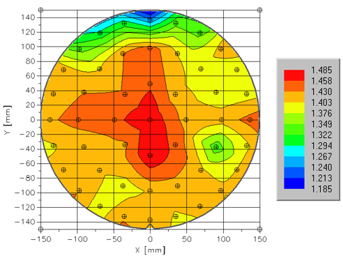
The Element G2 system is a high-speed epitaxial layer metrology and wafer/film composition control system for wafer makers, advanced logic, DRAM and 3D NAND.
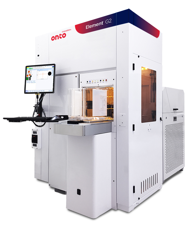
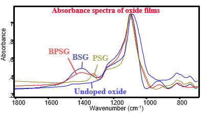
The Element G2 system is designed for wafer suppliers to perform high speed impurity mapping and epi thickness measurements. It combines transmission and reflection-based technology and when paired with advanced IR modeling capability, it offers a unique approach to dielectric composition and film thickness monitoring. With improved sensitivity and cutting-edge algorithms, the Element G2 system is a critical metrology tool widely used for monitoring dielectrics such as BPSG, FSG, H in SiN, and more. Machine learning helps eliminate the need for monitor wafers in dielectric measurement.
The system features a crisp 2mm circular IR spot, a high sensitivity interferometer and advanced pattern recognition. Equipped with a Class 1, five-axis dual-arm edge grip wafer handling system, the Element G2 system delivers high precision and high throughput, even at the edge of the wafer.
As your partner for innovative solutions, we’re always here for you.
Discover how our cutting-edge semiconductor solutions are engineered to meet your most complex challenges: delivering performance, reliability and innovation where it matters most.
"*" indicates required fields
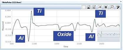
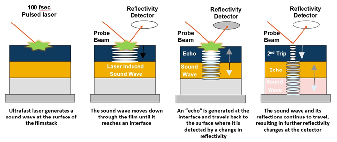
The Echo system utilizes picosecond ultrasonics to provide accurate, in-line, on-product metrology and materials characterization for semiconductor processes requiring metal thickness metrology, implant monitoring or thermal conductivity characterization on product wafers.
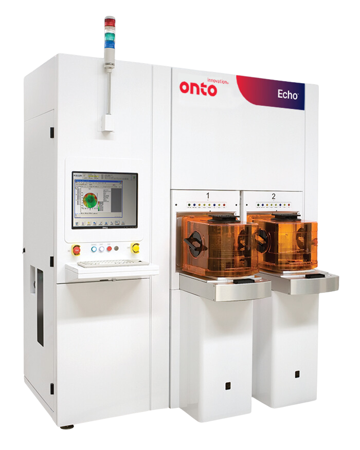
The Echo system is a comprehensive in-line metal film metrology tool designed for single and multi-layer metal film measurements in leading-edge logic, memory, advanced packaging and specialty semiconductor devices. Its innovative optics design extends the dynamic range for film thickness measurement from 50Å to 35µm on a single platform and offers extendibility to measure high aspect ratio advanced 3D NAND structures. The Expert Applications System (EASy™) software provides flexibility for developing user-defined algorithms to model complex multi-layer stacks.
The Echo system’s capabilities have been extended to include materials characterization. In addition to measuring the Young’s Modulus of low-k dielectric films in BEOL and amorphous carbon hard masks in 3D NAND, the Echo system includes proprietary electronics and algorithms for implant monitoring and thermal conductivity characterization. Its small spot size, combined with rapid measurements, enables full wafer mapping capabilities with 0.5mm edge exclusion, improving time to yield.

As your partner for innovative solutions, we’re always here for you.
Discover how our cutting-edge semiconductor solutions are engineered to meet your most complex challenges: delivering performance, reliability and innovation where it matters most.
"*" indicates required fields