
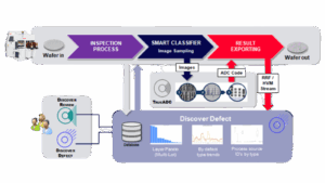
Discover® Defect Software
Integrated defect management system that works seamlessly with Onto tools and your entire enterprise, bringing data together for greater visibility and cleaner operation.

If you’ve been following the evolution of advanced packaging, you know that the industry is pushing boundaries like never before. From high-performance computing to industry-upending AI devices, the demand for smaller, faster, and more powerful chips is driving innovation at every level.

As semiconductor manufacturers push the boundaries of performance and functionality—driven by high-performance computing and AI applications—chemical mechanical planarization (CMP) processes increase in intensity complexity.
New logic transistor designs, 3D NAND stacking, and DRAM integration introduce more CMP layers and tighter process windows. Traditional metrology approaches struggle to keep pace, especially with the need for high sampling rates, multiple control zones, and improved signal-to-noise ratios.

Onto Innovation’s Intelligent Line Monitoring & Control with Integrated Metrology offers a transformative approach to CMP process control.
By leveraging data feedforward from standalone metrology tools to integrated metrology systems, this solution enables real-time, AI-driven process optimization.
At the heart of this solution is the IMPULSE® V system, an advanced integrated metrology platform that connects with standalone tools like the Atlas® system and utilizes Ai Diffract™ modeling software.
This ecosystem enables the creation of hybrid reference models—combining standalone data and limited TEM measurements—to drive high-precision, high-throughput results.
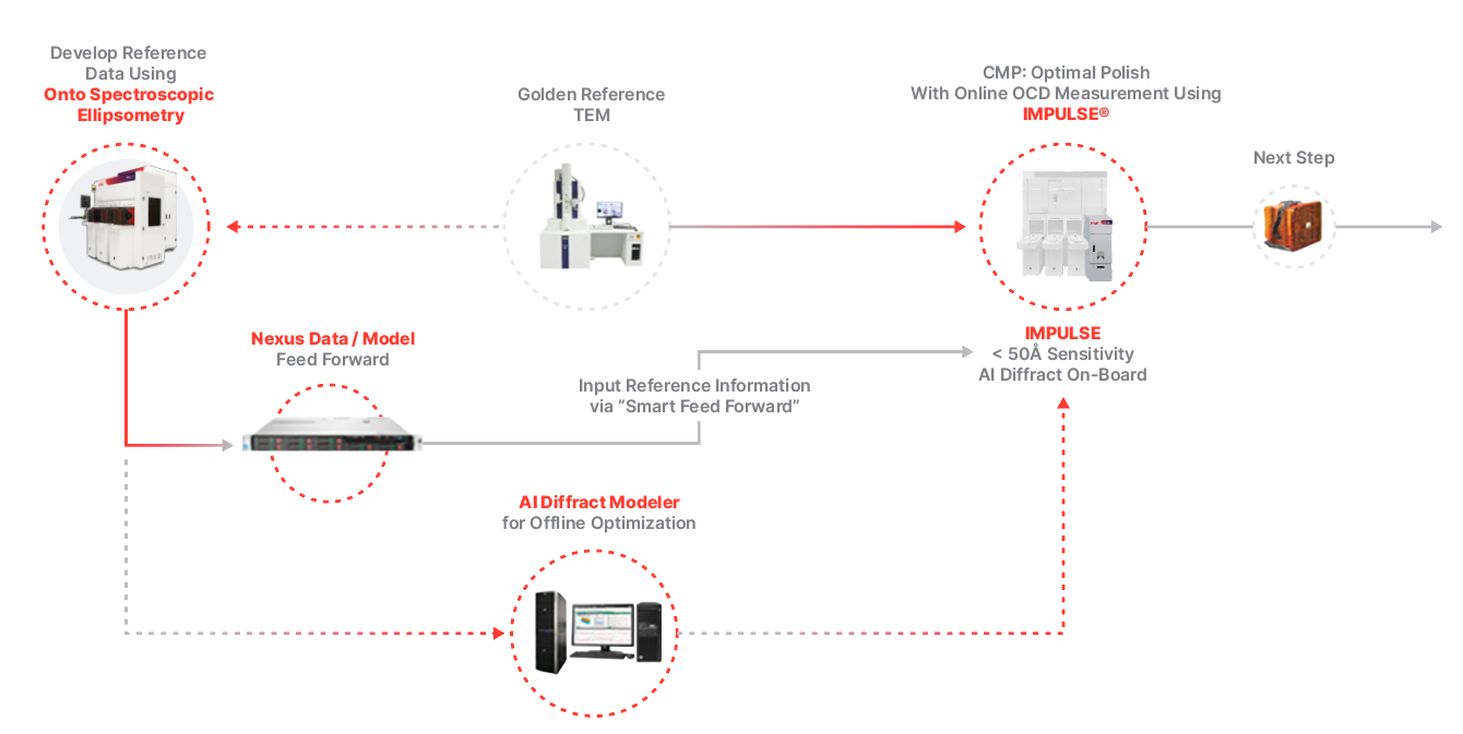
Accelerated Time to Solution: Feedforward of secondary parameters from standalone tools into IMPULSE system recipes enables faster model convergence and process tuning.
Improved Throughput: Skipping pre-measurements at the integrated metrology stage saves time without compromising accuracy
Reduced Cost and TEM Dependency: Hybrid reference modeling minimizes the need for extensive TEM data, reducing both cost and development time.
Enhanced Process Control: AI-driven analytics and model-based feedback improve excursion detection and process stability, leading to better Cpk performance.
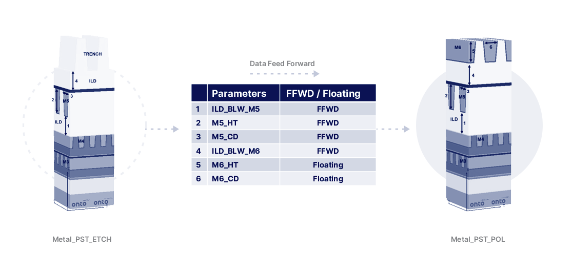
In a production environment, Onto Innovation demonstrated the power of feedforward data integration by correlating oxide loss measurements across standalone and integrated metrology tools. By feeding forward key parameters, the solution eliminated the need for redundant pre-measurements and improved correlation to reference data—delivering both time savings and enhanced process control.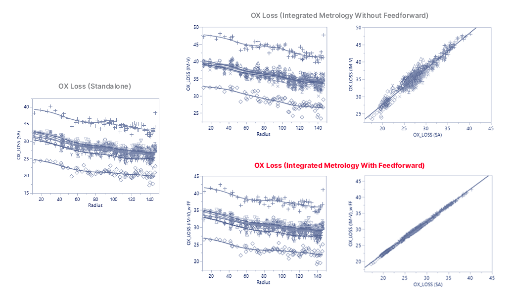

We’d love to connect with you.
Looking to learn more about our innovative solutions and capabilities? Our team of experts is ready to assist you. Reach out today and let’s starts a conversation about how we can help you achieve your goals.
"*" indicates required fields
As artificial intelligence (AI), high-performance computing (HPC), and advanced graphics processing continue to push the limits of memory throughput, the demand for high-bandwidth memory (HBM) has surged. These applications require faster access to massive datasets, driving the need for memory solutions that can deliver both speed and density without compromising power efficiency. HBM addresses this by stacking memory dies vertically and connecting them with ultra-fast interconnects. However, as data rates climb, traditional bump technologies—long relied upon as the primary interconnect method—are reaching their physical and performance limits.
Today, we stand at a pivotal moment in HBM interconnect technology. Hybrid bonding has emerged as one of the most talked-about technologies in advanced packaging. Promising finer pitches and superior electrical performance, hybrid bonding is generating excitement for its potential in high-performance applications. On the other hand, innovations in bump scaling are making bumps increasingly viable for a broad range of applications, beyond legacy and cost-sensitive applications. Despite these advancements, scaling bump pitch beyond 10μm and toward 2μm presents significant challenges. Maintaining uniformity and controlling bump height variation becomes more difficult, impacting yield and reliability. Meanwhile, taller HBM stacks, from 8-high to 24-high, require thinner dies, increasing the risk of die warpage and cracks during dicing.
Hybrid bonding is not without its challenges, too. At this scale, direct bonding demands plating uniformity and surface cleanliness to ensure reliable interconnects. In this article, we will examine the challenges facing bump and hybrid bonding technologies, the solutions these two technologies enable, and how they stack up compared to each other. We also will highlight how manufacturability, reliability, and process control evolve as pitches shrink and stack heights increase. To start with, we focus our attention on bumps, and then move on to hybrid bonding.
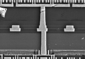
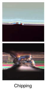
Microbumps play a critical role in enabling vertically-stacked HBM structures by serving as interconnects between dies, and dies to interposers or substrates. These bumps need to be uniform in height, properly aligned, and defect free (Figure 1).
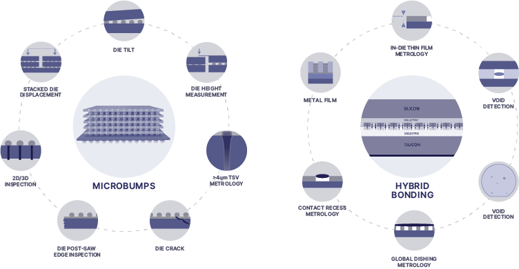
Figure 1. Interconnect challenges in microbump and hybrid bonding technologies.
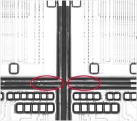
Inconsistent bump height in HBM can result from plating nonuniformity and process variability, and it negatively affects yield, reliability, and performance. Meanwhile, poor coplanarity can lead to mechanical stress, interconnect fatigue, or thermal cycling failures, while inconsistent contact can degrade signal integrity and power delivery. Misalignment during flip-chip bonding can result in open or short circuits. Given the breadth of these challenges, manufacturers should focus on identifying issues after the plating step and before the reflow step. After all, if you have a plating problem but move onto reflow, it will be too late to fix the problem.
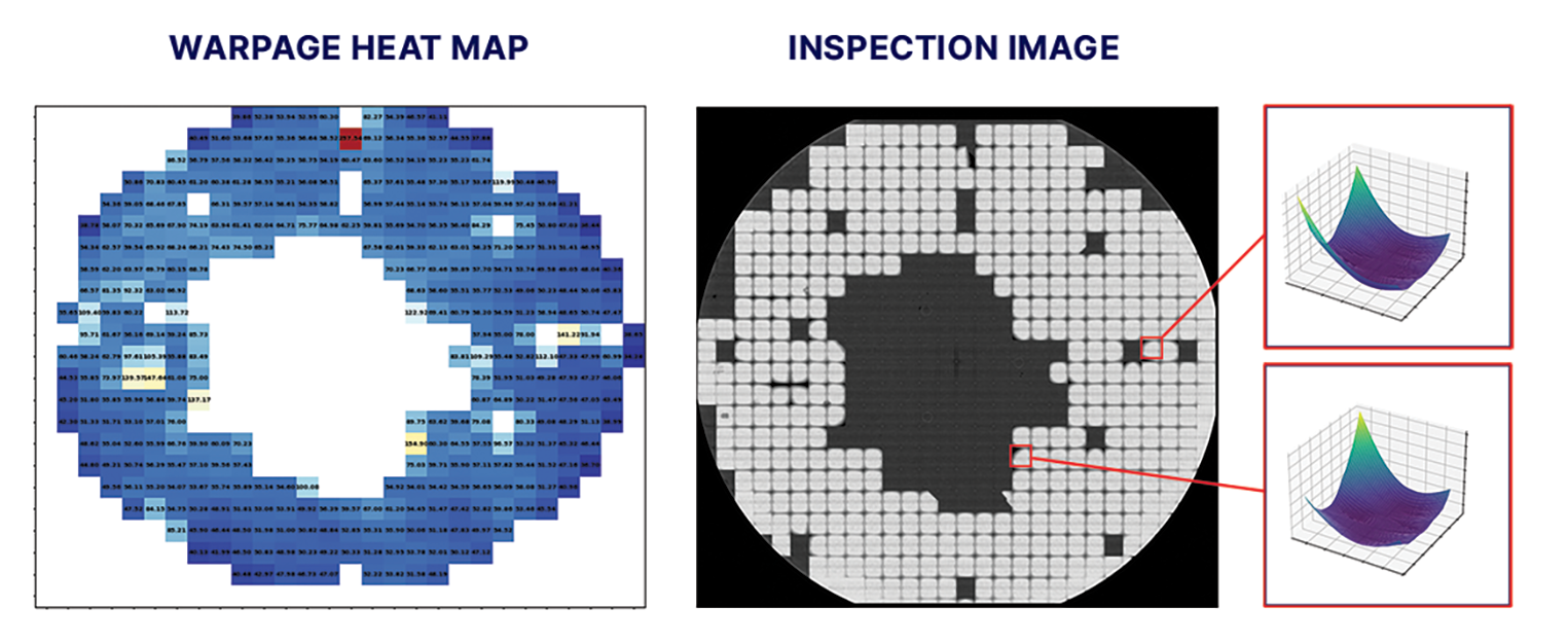
With the number of layers in an HBM stack continuing to rise, addressing die warpage becomes even more essential (Figure 2). First of all, die warpage significantly compromises stack alignment and bonding quality. This is especially critical given the extremely tight tolerances of HBM. In addition, warpage can also result in voids, opens, and a host of other issues leading to electrical failures, mechanical stress and cracking, yield loss, and thermal performance degradation, resulting in overheating and reduced performance. Meanwhile, organic residue can result in surface contamination, voids and delamination, oxidation and corrosion, and diminished yield and reliability.
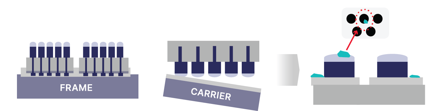
Properly identifying cracks and alignment errors in bumps poses another challenge (Figure 3). Cracks often occur during the dicing and backside grinding process and can break the electrical path, leading to open circuits. They often propagate due to thermal cycling, especially in materials with different coefficients of thermal expansion (CTE), weakening the bump structure. Even if initially functional, cracked bumps are prone to failure under thermal or mechanical stress during operation.
Misalignment of dies is another problem. It is often caused during the pick and place step due to the lack of backside patterns. This lack of patterning makes it difficult to tell if overlay is accurate—this is something with which automated optical inspection systems struggle.
The key reason hybrid bonding has emerged as a new technology for HBM is simple: improved interconnect density and smaller package sizes. To begin with, hybrid bonding enables finer interconnect pitches, less than 10μm, allowing for more I/O terminals in a smaller area. This increased density translates directly into higher bandwidth and improved overall performance.
Traditional bump-based stacking introduces gaps of about 30μm between dies. Hybrid bonding offers direct Cu-to-Cu connections, thereby achieving near-zero spacing between dies, significantly reducing overall package thickness and offering lower resistance and better thermal conductivity than bump-based methods. This improves signal integrity, reduces power consumption, and enhances heat dissipation, all of which are critical for HBM.
Finally, hybrid bonding supports several configurations: wafer-to-wafer, die-to-wafer, and die-to-die, offering flexibility in manufacturing and integration. This adaptability is vital for scaling HBM technologies across different applications and performance tiers.
With our introduction to bumps and hybrid bonding complete, we now turn to a comparative discussion of these two technologies, building on earlier points and exploring new ones.
Bumps have several advantages over hybrid bonding. As a mature technology, they are widely used and well understood in the industry, are compatible with existing flip-chip and underfill processes, and are scalable for moderate density. The cost of bump technologies is lower than hybrid bonding technologies. Bumps, however, have a number of disadvantages compared to hybrid bonding. The most significant of which are the pitch limitations of bump technologies, which struggle at pitches below 10µm due to challenges in plating uniformity and solder reflow. Bumps also require underfill, which can introduce stress and complicate thermal management.
Despite the limitations noted above, bump technology continues to evolve. Leading suppliers of bump plating systems project a continued downscaling of bump dimensions, with diameters decreasing to the 4µm-5µm range and heights dropping as low as 1µm to 2µm. At a 10µm pitch, the lateral footprint remains sufficient to support the high-density I/O requirements of advanced memory architectures. Concurrently, the reduced bump height enables vertical integration of up to 16 stacked HBM dies within the 775µm maximum package height defined by Joint Electron Device Engineering Council (JEDEC) standards. Consequently, bump interconnects remain a viable and scalable solution for next-generation HBM, and major manufacturers are maintaining substantial R&D investments in bump technology.
Hybrid bonding, while promising, presents its own set of challenges. In addition to being more expensive than traditional bump technologies, hybrid bonding may require manufacturers switching from bump technology to purchase new equipment and adopt new process flows. In addition, hybrid bonding is especially sensitive to particles and organic residues; for example, even 1µm particles can cause defects. Such residues can prevent proper contact, trap gases or moisture, and lead to void formation during bonding. These voids can cause delamination or incomplete bonding, reducing mechanical integrity and electrical continuity.
Process control for hybrid bonding is challenging, but these obstacles can be addressed by employing a suite of advanced metrology and inspection technologies, as well as analytic software solutions.
High-speed, sub-micron inspection can be used to detect surface anomalies such as particles, residues, and backside and edge defects (Figure 4). This ensures that bonding surfaces are clean and defect-free before the bonding process begins. As for overlay misalignment, the capability to measure wafer topography and alignment with sub-micron precision enables accurate die placement and reduces the risk of misalignment during bonding. As for voids, a non-contact, immersion-free acoustic metrology technology capable of detecting voids down to 1µm is effective at identifying bonding defects that could lead to electrical or thermal failures. Furthermore, a sub-micron inspection system can be used to detect defects like cracks and delamination caused by thermal or mechanical stress.
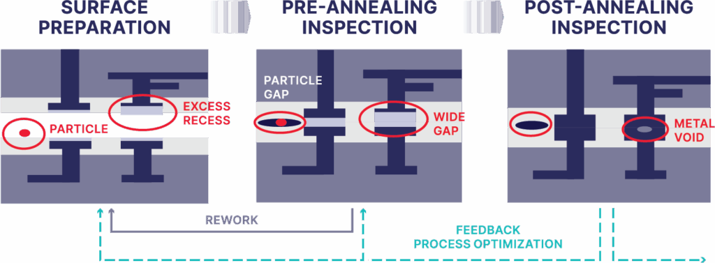
Figure 4: Hybrid bonding metrology and inspection challenges.
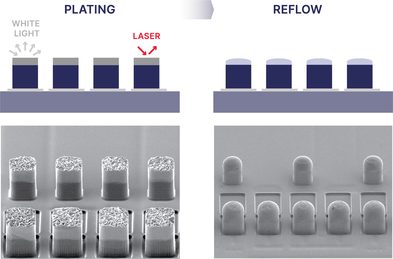
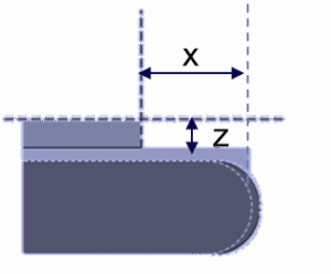
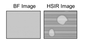
In the case of bump-based interconnects, the ability to measure Cu-to-Cu bump height down to 1.5μm will be key. However, several of today’s technologies employ white light illumination technologies that are unable to properly identify defects on these exceptionally small Cu pillars before reflow (Figure 5). After reflow, the bump shape is very clean and very smooth; but before reflow and after plating, the Cu is very rough. Typically, when white light hits a very rough surface, the light randomly scatters. However, an inspection system that uses a coherent wavelength laser technology can overcome this challenge.
In addition to the points noted above, an integrated system using analytical software can be used to detect errors and provide real-time defect analysis and statistical process control. Software can be used to provide in-line process control insights about defects and offer actionable corrections and is capable of handling millions of bumps per wafer, with each bump generating multiple data points. This integration helps manufacturers trace contamination sources and optimize cleaning steps, improving bonding reliability.
New technologies are actively being adopted for interconnect control in HBM. In the case of bump process control, the sector is moving toward smaller dimensions, 12µm to 4µm in high-volume manufacturing and below 2µm in R&D. Meanwhile, hybrid bonding is gaining traction due to its ability to support higher interconnect density and performance. This shift is driving the adoption of advanced inspection and metrology techniques, including an opto-acoustic void detection technology capable of detecting voids down to 1µm—a critical point for yield in HBM production.
Foundries are integrating bump inspection and metrology tools into their advanced packaging lines, especially for custom HBM and logic solutions. At the same time, hybrid bonding adoption is accelerating, particularly in the case of chiplet-based and heterogeneous integration strategies.
This year, R&D is expected to push microbump pitch to 6µm and hybrid bonding density to 60 interconnects/mm². In the coming years, microbump pitch may scale down to 3µm, while hybrid bonding density could reach 100 interconnects/mm². Long term, hybrid bonding is projected to become a mainstream interconnect technology, surpassing microbumps in many advanced applications, with densities reaching 150 interconnects/mm² and microbump pitch shrinking to 1.5µm.
As it stands today, there is no single solution for all HBM use cases. Instead, manufacturers may adopt an approach leveraging both bump and hybrid bonding, supported by a comprehensive process control strategy that integrates metrology, inspection, and advanced analytics.
Damon Tsai is the Senior Director of Product Marketing, Inspection, at Onto Innovation, Milpitas, California. He joined the company in 2018 and has extensive experience in inspection and metrology, with a specialized focus on semiconductor FEOL, advanced packaging, OSAT, and specialty markets like RF, Power, and CIS.
Woo Young Han is Product Marketing Director, Inspection, at Onto Innovation, Richardson, Texas. He joined Onto Innovation in 2000 and holds an Electrical Engineering degree from the University of Toronto.
We’d love to connect with you.
Looking to learn more about our innovative solutions and capabilities? Our team of experts is ready to assist you. Reach out today and let’s starts a conversation about how we can help you achieve your goals.
"*" indicates required fields
AI data centers are pushing for higher density in high-bandwidth memory. Today, the maximum number of layers that can be stacked is 8, but that increases to as many as 24 layers by 2030. The big challenge will be in the interconnects, and making sure the microbumps align. At 16 layers, the bump pitch will be less than 10 microns, and the dies will be thinner. Damon Tsai, head of product marketing for inspection products at Onto Innovation, talks with Semiconductor Engineering about how to reduce stress that can cause warpage, how HBM architectures will need to change, and what happens when hybrid bonding and co-packaged optics are added into these devices.


We’d love to connect with you.
Looking to learn more about our innovative solutions and capabilities? Our team of experts is ready to assist you. Reach out today and let’s starts a conversation about how we can help you achieve your goals.
"*" indicates required fields
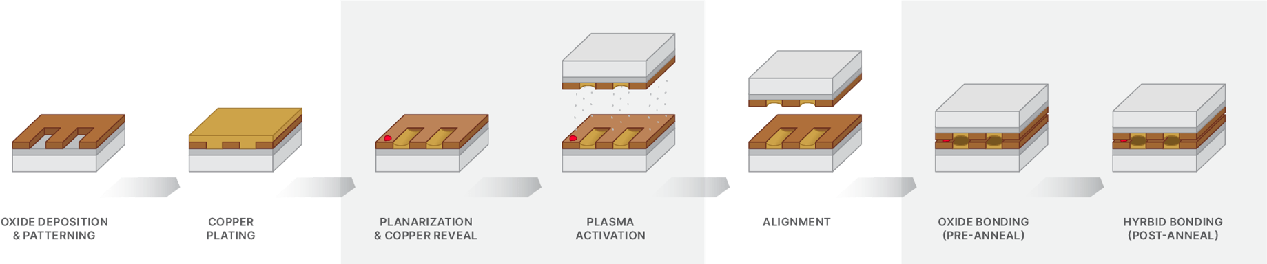
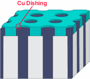
As demand grows for high-performance computing (HPC) and AI-driven applications, manufacturers are turning to hybrid bonding to enable the ultra-dense 3D integration required for next-generation chip architectures.
This advanced packaging technology presents significant process challenges. Surface preparation must be precisely controlled to eliminate particles, excess recess, and copper pad dishing, all of which can compromise bond quality. During pre-annealing, particle-induced gaps and wide bonding gaps can prevent proper wafer contact. Post-annealing, the formation of dielectric and metal voids introduces further risks to electrical performance and long-term reliability. If not carefully managed, these issues can lead to increased defectivity, reduced yield, and degraded performance in HPC and AI systems where reliability and speed are critical.
Source: AMD 3D V-Cache with TSMC SoIC 3D Packaging reverse engineering & costing report, Yole Group, 2022
Hybrid bonding reliability starts with robust process control. Monitoring topography and detecting particles, cracks, and voids help identify defects early. Measuring copper pad dishing offers insight into surface conditions and planarity. Tight control during pre-bonding steps enables potential rework before permanent defects occur.
The following examples highlight key metrology and inspection techniques that support more consistent hybrid bonding outcomes.
The native integration of the Discover software platform boosts tool throughput and enhances inspection quality by capturing more defects of interest. It provides a complete reduced review solution utilizing advanced machine learning (ML) and artificial intelligence (AI) technologies, customized to meet unique customer needs.
Optimized Image Capture for Inspection Tools
Discover software enhances inspection quality and tool throughput by optimizing the image capture sample plan.
AI-Powered Automatic Defect Classification (TrueADC Software)
Integrated AI-based classification improves device quality and yield, driving fab efficiency and productivity.
Streamlined Review Software
Reduced review best practices improve operator productivity, enhance engineering review quality, and shorten review time.
Advanced Defect Analytics
Comprehensive inline wafer/panel monitoring enables automatic alarm notifications, detailed reports and Out-of-Control Action Plans (OCAPs).
Defect Source Analysis
Enables actionable process feedback to improve manufacturing outcomes.
Automated Business Analysis with Report Server
Boosts engineering productivity by up to 25% and supports multiple production report formats.
Machine Learning-Based Pattern Detection
The Discover Patterns software module proactively identifies wafer-level systematic yield-limiting issues and classifies them for analytics, enabling both process feedback and feedforward.
Centralized Defect & Metrology Management
Built on a scalable Big Data and high-availability architecture, this solution supports advanced applications such as high volume manufacturing (HVM) bump metrology, capable of handling wafers with over 100 million bumps.


As your partner for innovative solutions, we’re always here for you.
Discover how our cutting-edge semiconductor solutions are engineered to meet your most complex challenges: delivering performance, reliability and innovation where it matters most.
"*" indicates required fields
A suite of OCD modeling software and computing hardware that enables the full capability and connectivity across all Onto OCD and thin film metrology systems, including Atlas, Aspect, Iris and IMPULSE systems.
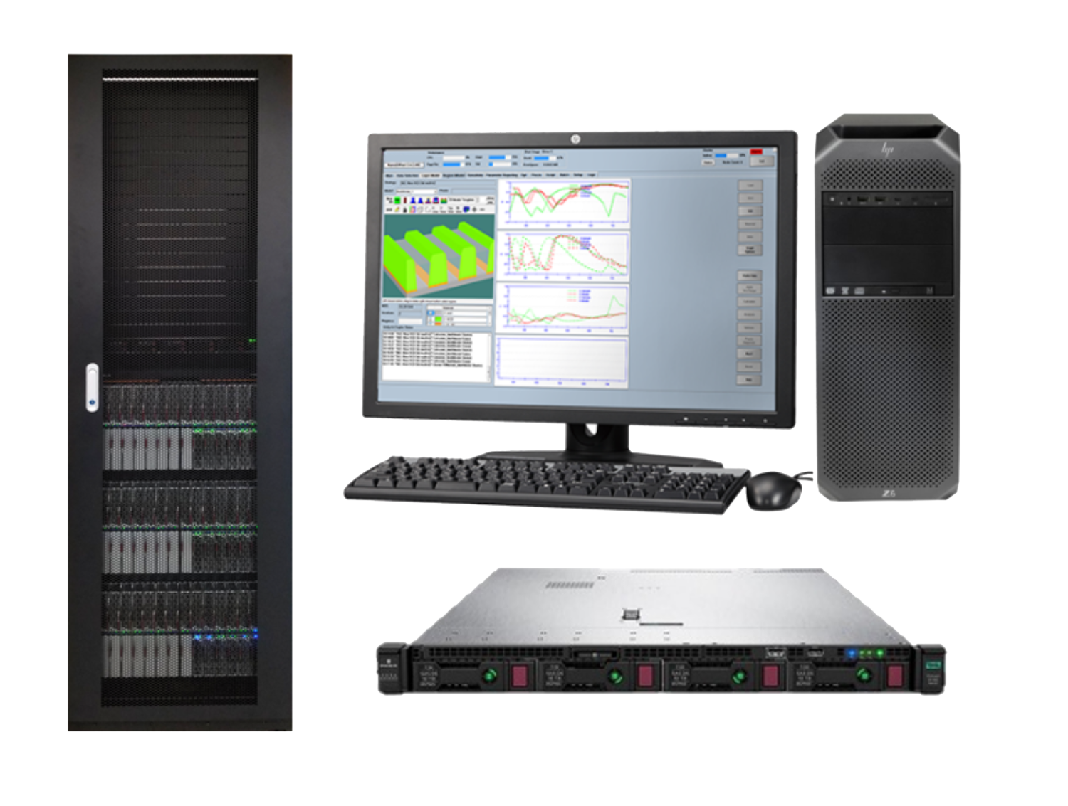
Onto Innovation’s OCD technology offers powerful modeling and computing packages to support various phases of film and OCD measurement setup, data management, and fleet management. These capabilities include model building, runtime data analysis, system calibration, data analytics, data connectivity and management, spectrum management and fleet matching.
Onto OCD solutions consist of several modeling and computing components, including Ai Diffract™ modeling software, runtime onboard computer, offline modeler, offline model building clusters, and recipe & data management server. Each component seamlessly extends OCD capabilities to Onto’s standalone and integrated metrology systems, providing end-to-end capabilities from offline recipe support and development to fab-wide networking and connectivity for easy fleet management.
Ai Diffract software is a powerful modeling, visualization and analysis software with an intuitive 3D modeling interface to simplify the building and visualization of today’s most complex semiconductor devices. It offers OCD modeling and advanced machine learning capabilities, next-generation real-time regression, offline sensitivity analysis tools and comprehensive GUI and structure input for true multi-variant modeling. Ai Diffract software’s proprietary fitting algorithms enable fast and accurate calculations for signal processing, helping ensure high fidelity model-based measurements. Automation features for spectral fitting, recipe optimization, and sensitivity analysis offer great user productivity. The first-in-market AI-guided engine synergizes physics-based modeling and machine learning to deliver the most robust solution with quick time to solution.
Ai Diffract Modeler is the offline analytical engine that allows users to create and edit recipes offline. It supports multiple users and can connect to Ai Diffract cluster for high intensity computing.
Ai Diffract Onboard is the on-tool runtime engine that maximizes tool throughput for complex use cases. It ensures rapid analysis without interfering with system operation or impacting throughput.
Ai Diffract Cluster is an enterprise scale computing server deployed for offline recipe development or in-line real-time regression. Optimized to support the workload of Ai Diffract software analysis, it scales based on fleet size, recipe numbers, and computing intensity.
Recipe Distribution Server (RDS) / Nexus Servers is a fab-wide networking and server system for fleet management and connectivity. RDS/Nexus servers provide connectivity and support to Ai Diffract recipe management and distribution, data/spectrum feed-forward and feedback, spectrum management, and fleet management.


As your partner for innovative solutions, we’re always here for you.
Discover how our cutting-edge semiconductor solutions are engineered to meet your most complex challenges: delivering performance, reliability and innovation where it matters most.
"*" indicates required fields