
Dragonfly® G3 System
Highly configurable, automated, high speed 2D inspection and 3D metrology for inline process control in advanced packaging, specialty and front-end OQA.
In a world where high-bandwidth memory, GPUs, and advanced AI packages are all the rage, it is easy to forget the important role specialty devices play.

May 5 — May 7, 2026
Onto Innovation is a proud exhibitor at SEMICON Southeast Asia.
In a world where high-bandwidth memory, GPUs, and advanced AI packages are all the rage, it is easy to forget the important role specialty devices play. These unsung heroes of modern life perform critical functions across a wide range of industries, including automotive, telecommunications, data centers, emerging AI hardware ecosystems, and consumer electronics, just like the smartphone in your hands, on your desk, or in your pocket. You know, the little pocket computer that never leaves your side.
And with new functions being added to consumer electronics with each new generation, the demand for specialty devices is on the rise. On the other end of the spectrum, manufacturers are facing an increasing number of challenges brought on by the growing complexity of these devices. Examples of this include SiC and GaN power devices, MEMS sensors, RF filters, photonics, and CMOS image sensors. We will cover all of these device types in this blog, the second in our three-part blog The Specialty Device Surge.
As discussed in part one of our series, the specialty segment is moving to larger wafer sizes. Not only does this transition promise higher throughput and improved economies of scale, it introduces new manufacturing and process control challenges, many of which are unique to each device category. Why? Each type of specialty device relies on unique materials, architectures, and process steps.
Across the industry, this complexity shows up in different ways. MEMS devices rely on a variety of materials or key processes depending on their core function: thick piezoelectric films, suspended mechanical structures, and near‑perfect plasma‑etched sidewalls, each requiring highly specialized deposition and metrology techniques. CIS manufacturing spans multiple bonded layers—pixel, CMOS, and microlens—each with its own set of defect, CD, and uniformity challenges that directly shape image quality. Power devices such as SiC and GaN introduce further hurdles: crystalline defects, trench‑shape control, epitaxial thickness uniformity, and surface‑quality demands that grow more difficult as these materials scale toward larger wafers. Photonics and co‑packaged optics push complexity even further, requiring precision across waveguides, doped films, microlenses, lasers, and the multi-die assembly process that integrates them into a single high-bandwidth module.
However, all these technologies share a simple truth: achieving high-volume production depends on advanced metrology, intelligent inspection, and tightly integrated feedback and feed‑forward control. Combined, these tools allow device makers to stay inside increasingly narrow process windows as specialty devices scale, diversify, and enter high‑volume production.
But first, let’s dive into the challenges facing specialty devices. We will begin by focusing on MEMS.
MEMS
The top five MEMS device types are pressure sensors, gyroscopes, accelerometers, microphones, and surface acoustic wave (SAW)/bulk acoustic wave (BAW) radio frequency (RF) MEMS. These are known as the Billion Dollar Club. And with good reason. Each of these devices is responsible for sales in excess of $1 billion per year. Impressive.
MEMS devices rely on either a unique material or unit process to deliver their core functionality. In the case of pressure sensors and microphones, the unique material is typically polysilicon or dielectric membranes or piezo films, which require very specific chemical or physical vapor deposition techniques to achieve the required film thickness and orientation to maximize the piezo coefficient for the material. For gyroscopes and accelerometers, the device relies on the formation of what are called interdigitated comb fingers; these capacitors rely on precise plasma etch techniques to deliver vertical side walls. However, any tilt can result in poor device operation.
Finally, there are the class of RF filter devices known as BAW devices. These devices rely on precisely deposited piezo films of either AlN or scandium doped aluminum nitride. In BAW devices, thickness and film orientation control the frequency of operation; as such, thickness uniformity across the entire wafer is essential keeping each device operating at the required frequency.
CMOS Image Sensors (CIS)
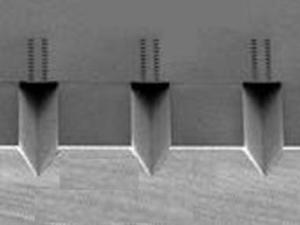
Today’s CIS devices are anywhere from 6µm to 10µm tall, with pixels in the image layer and separated from one another by approximately 100nm-wide isolation trenches.
Pixel formation relies on several dopant implant steps. The isolation trenches have sidewalls specifically engineered to increase total internal reflection, thereby increasing the light capturing efficiency of the pixel, and minimize so-called dark noise (the movement of electrons within the pixel when no light is present). The latter typically involves increasing the work function of the materials along the sidewalls of the isolation trenches.
In the formation of a pixel imager, multiple challenges, from epitaxial layer thickness and dopant uniformity metrology to isolation trench defect inspection and CD and shape metrology, exist. Each challenge must be addressed to create the perfect pixel for imaging.
Several unique metrology and inspection steps are needed for each layer. Layer 1 of the CIS is the pixel layer, layer 2 is the CMOS layer which is usually hybrid bonded to the pixel layer, and layer 3 features the microlens array which is either bonded or manufactured directly on the pixel wafer.
SiC and GaN Power Devices
In recent years SiC has seen a tremendous surge in popularity given its use for switching high voltages in EV motors. Today, SiC is in production at 200mm. However, some manufacturers have started to produce 300mm SiC wafers for applications that take advantage of the material’s unique thermal conductivity.
Inspection and metrology play key roles in the production of SiC power devices. First of all, inspection is used to identify latent or killer crystalline defects in the initial substrate and subsequent epitaxial SiC layers. Then, regular particle defect inspection and all-surface inspection is performed to catch additional defects on the edge or backside of the wafers. Multiple particle defect inspections are carried out throughout the remainder of the high-volume manufacturing process.
Now on to metrology. The ability to conduct accurate measurements plays a key role in understanding the thickness, dopant concentration, and uniformity of the epitaxial layers grown on the initial substrate. The importance of metrology does not end there. Across the remainder of the process flow, CD metrology and trench shape metrology play a part in ensuring device yield and performance.
Unlike SiC, GaN technologies migrated to 300mm wafers earlier. For GaN power devices, the challenge involves identifying crystalline defects, surface roughness metrology, AlGaN layer homogeneity, and CD metrology.
The key need for original equipment manufacturers supporting customers in this segment is the ability to deliver inspection and metrology technologies that can handle these materials and associated wafer thicknesses, while also performing necessary inspection or metrology steps at cost-of-ownership price points for power devices. After all, these technologies need to offer manufacturers economically viable alternatives to ever-improving silicon power devices.
Photonics and Co-Packaged Optics
Photonics technologies have been around for decades, but they have evolved with the times. Now you can find photonics in a growing number of applications, including laser printing and xerography, facial recognition, and several telecommunication-based applications. Today, however, we’re seeing a new demand driver for this technology: AI.
Current AI devices communicate via standard metal traces. However, the increasing bandwidth requirements of AI chipsets and the power dissipation incurred from the use of copper wiring within data centers have combined to create a demand for a high-speed technology that consumes little power: silicon photonics.

Figure 1: Left to right, examples of V-grooves, basic waveguide geometry, and refractive and diffractive micro-lens structures. Each physical device brings with it its own set of key inspection and metrology requirements.
Silicon photonics replace these metal traces with optical waveguides that use light, not electrons, to carry information. In the case of co-packaged optics (CPO) which are directly integrated with chips, photonics provides ultra-high-bandwidth, low-power, light-based data transmissions. CPO combines laser sources with waveguide-based silicon chips, micro-lenses, and opto-electronic converters in a package that fits neatly on the modern panel level AI package. This one small module represents the cumulative challenges of multiple manufacturing segments under the umbrella of photonics and optics. Addressing these challenges requires V-groove inspection and metrology, waveguide metrology, micro-lens inspection and metrology, and a number of other areas including dopant uniformity (Figure 1). In the end, the ultimate success of any given CPO module relies on the assembly of all the die that go into it.
Conclusion
Whether the subject is MEMS structures demanding near perfect sidewalls, CIS stacks spanning multiple bonded layers, power devices pushing wide-bandgap materials to their limits, or photonics and co‑packaged optics, the common challenge manufacturers face is control. Across every specialty device category, success hinges on advanced metrology and inspection solutions that can precisely measure what matters most—shape, thickness, uniformity, defects, and material properties—at high throughput and low cost.
In the final blog of this three-part series, we’ll shift our attention from the challenges facing specialty devices to their solutions. We hope you will join us to learn more about these unsung heroes of modern life.
Christopher Haire is a marketing content specialist at Onto Innovation and a former business journalist.

We’d love to connect with you.
Looking to learn more about our innovative solutions and capabilities? Our team of experts is ready to assist you. Reach out today and let’s starts a conversation about how we can help you achieve your goals.
"*" indicates required fields
Specialty devices are the unsung heroes of modern life. For many in the semiconductor industry today, the spotlight is on the SiC and GaN power devices used in automotive, green energy, fast-charge consumer electronics (CE), and high-performance computing (HPC) applications (Figures 1 and 2).
However, specialty devices are more than just power devices. They are a broad class of semiconductor components delivering a variety of functions across multiple industry segments, including microelectromechanical systems (MEMS) in automobiles and CE to radio frequency (RF) filters for 5G/6G communications.

Figure1: Planar SiC MOSFET and trench SiC MOSFET

Figure 2: Vertical GaN and GaN on Si high electron mobility transistor (HEMT)
Photonics are another type of specialty device making industry waves. Previously viewed as something of a dark horse in the specialty sphere, photonics have made a comeback. Today, photonics are being used for 3D sensing in multiple CE applications such as smartphone user verification and 3D imaging, automotive applications in which scanning lasers are used in advanced driver assistance systems (ADAS); and telecommunications applications where photonics have long been used as optical transceivers supporting the conversion of copper wiring to optical fiber communications in data centers. While these applications and others exist for photonics, the killer photonics application is shaping up to be co-packaged optics (CPO), which enables optical communications directly from packaged XPU devices supporting AI applications.
When it comes to the broad category of specialty devices, nearly all of them are either manufactured on or previously manufactured on 150mm or 200mm wafers. However, specialty devices are moving to larger wafer sizes, either 200mm or 300mm depending on device type.
With many specialty devices scaling to larger wafer sizes, the semiconductor industry faces new challenges in process control. After all, specialty devices are known for delivering specialized features or capabilities based on a unique process step or material that often requires a customized inspection and metrology solution.
To optimize the manufacturing process, real-time process control —powered by data analytics and software —has become an indispensable requirement in specialty device fabrication. To scale specialty technologies for high-volume manufacturing, manufacturers need integrated solutions and specialty-focused platforms offering flexibility, precision, and automation across multiple wafer sizes.
In this three-part blog series, we will begin by discussing one of the most important trends in specialty devices, the transition to larger wafer sizes and what this means for specific devices. The following blogs will focus on the challenges facing the manufacturing of specialty devices and the solutions addressing these challenges.
From Niche Applications to Mainstream Products
Originally, specialty devices were referred to as More-than-Moore devices because the use of these devices went beyond the simple node scaling of traditional CMOS devices. They also were being enabled by one or more “specialty” materials or process steps. In fact, the semiconductor industry did not start using the term “specialty devices” until these devices transitioned from niche applications to mainstream products and high-volume production.
But what exactly are the benefits of these specialty materials? Let’s consider the case of specialty power devices.
The compound semiconductors used in power specialty devices, SiC and GaN, can handle high voltages more efficiently than traditional Si. They provide the ability to switch high voltages in increasingly smaller areas and at higher speeds than their silicon-based counterparts. They do this without the elaborate cooling that would otherwise be required. As these materials scale to larger wafer sizes, they necessitate upgrades in wafer fabrication equipment, inspection, and metrology tools.
Transitioning Wafer Sizes
Specialty devices have long been the domain of 150mm and 200mm wafers, with CMOS image sensors (CIS) and power management devices being the exception. That’s all changing.
On the compound semiconductor front, the high demand for GaN-based high-power, fast-switching technologies is motivating a wafer size transition from 200mm to 300mm while SiC power devices are transitioning from 150mm to 200mm in high-volume manufacturing. In addition, photonics technologies now span wafer sizes of 150mm to 300mm, and MEMS devices are offered at 300mm.
As more specialty device technologies move into high-volume manufacturing, we can expect to see a greater demand for 300mm silicon, glass, and compound semiconductor-based wafer applications. However, this transition to larger wafer sizes introduces unique challenges for each specialty device type. These devices and their challenges include:
MEMS: Larger substrates and diverse materials (Si, glass, thick metals) require tighter process control of etch depth and CD, feature height across bowed or warped wafers, and surface roughness.
SiC Power: As SiC power moves to 200mm, inspection and metrology must expand sampling, deal with increased crystal defects, and support device architecture transitions profiling complex trench MOSFETs (e.g., top/bottom CD) without killing throughput. Insufficient sampling on larger wafers creates blind spots that hurt yield and cost of ownership.
GaN Power: Moving GaN to 300mm wafers increases within-wafer variation, requiring more measurement points and precise control of trench/HEMT critical dimensions to maintain uniform performance, while dealing with increasingly brittle and bowed or warped materials.
Photonics and CPO: Co-packaged optics require metrology tools designed for die-to-die and wafer bonding (voids, Cu dishing, film variation), sub‑micron alignment, and warpage, which affects optical coupling on larger wafers and multi‑die assemblies.
CIS: CIS stacks drive high sampling density for overlay and CD uniformity. These stacks require integrated chemical mechanical planarization metrology and analytical tools to catch excursions quickly as die counts and wafer diameters increase.
To meet these challenges and others, manufacturers need upgraded metrology and inspection tools, many of which will come from suppliers with a long-standing relationship with specialty technologies. These suppliers are best prepared to meet the wafer handling, on-wafer materials, and cost-of-ownership requirements that have become synonymous with the specialty device markets.
Conclusion
The emergence of specialty devices as a vibrant market of their own is driven by the increasing complexity and functionality of end products. Even in mature markets, such as smartphone and automotive, manufacturers continue to innovate by adding new features, which, in turn, fuels demand for additional specialty devices.
In our next blog, we will further explore the many challenges facing each type of specialty device. We hope you join us as we discuss those challenges and, in part three of our series, the solutions that are available in the specialty space today.
Christopher Haire is a marketing content specialist at Onto Innovation and a former business journalist.
We’d love to connect with you.
Looking to learn more about our innovative solutions and capabilities? Our team of experts is ready to assist you. Reach out today and let’s starts a conversation about how we can help you achieve your goals.
"*" indicates required fields
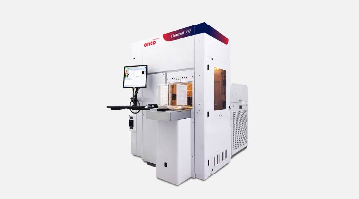
The Dragonfly G5 system is engineered for inline process control of leading-edge advanced packaging technologies. As the latest generation pattern inspection system in the Dragonfly series, it delivers unparalleled accuracy in detecting submicron defects and performing high-resolution 3D measurements.
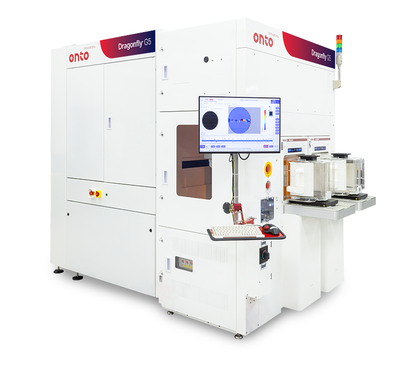
Designed to meet the demands of advanced semiconductor technologies, the Dragonfly G5 system is purpose-built to deliver high-performance, reliable inspection and metrology across complex heterogeneous integration processes. Leveraging next generation high speed line scan 2D imaging and custom-engineered objectives, the system achieves over 3X throughput improvement compared to its predecessor, with submicron sensitivity down to 150nm.
Continuing the legacy of innovation, the Dragonfly G5 system introduces a multi-angle illumination channel that significantly improves signal-to-noise ratio for faint defect detection. Combined with powerful AI-driven algorithms, it enhances both the detectability and classification of critical, yield-impacting defects–empowering fabs to maintain quality and accelerate time-to-yield.
The Dragonfly G5 system expands process control flexibility for wafer-to-wafer and die-to-wafer bonding by integrating high-speed IR imaging to detect sub-surface defects. It incorporates the latest generation of 3Di™ technology, extending bump height metrology capabilities to support next-generation microbumps essential for 3D integration. This enables additional inspection and metrology touchpoints across increasingly complex packaging architectures.


Hybrid bonding enables ultra-dense 3D memory interconnects with up to 1,000x more connections than microbumps. Achieving high yield requires stringent process control, including monitoring topography and detecting particles, cracks and voids. Measuring dishing in copper pads provides valuable insight into surface conditions. Together, these process control insights contribute to improved device reliability and performance.

As demand grows for high-performance computing (HPC) and AI-driven applications, manufacturers are turning to hybrid bonding to enable the ultra-dense 3D integration required for next-generation chip architectures. This advanced packaging technology presents significant process challenges. Surface preparation must be precisely controlled to eliminate particles, excess recess, and copper pad dishing, all of which can compromise bond quality. During pre-annealing, particle-induced gaps and wide bonding gaps can prevent proper wafer contact. Post-annealing, the formation of dielectric and metal voids introduces further risks to electrical performance and long-term reliability.

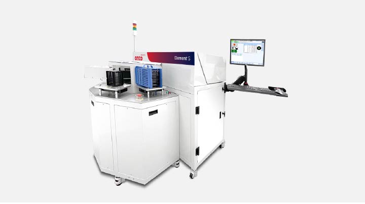
The Iris S system is a versatile platform solution for the advanced packaging and specialty market, supporting 150mm, 200mm and 300mm wafers. It provides thin and thick film, OCD and wafer bow and film stress measurements.

The IMPULSE V system helps to advance CMP processing with enhanced wavefront technology and AI-driven analytics, delivering over 2X precision improvement and faster solutions, crucial for next-gen semiconductor manufacturing demands.

The Dragonfly G5 system is engineered for inline process control of leading-edge advanced packaging technologies. As the latest generation pattern inspection system in the Dragonfly series, it delivers unparalleled accuracy in detecting submicron defects and performing high-resolution 3D measurements.

The Aspect System is a revolutionary in-line, non-destructive infrared optical critical dimension (IRCD) system measuring Z-dimension profiling of high aspect ratio structures to enable critical process control. It meets the needs of leading-edge customers with its high speed and process coverage.
As your partner for innovative solutions, we’re always here for you.
Discover how our cutting-edge semiconductor solutions are engineered to meet your most complex challenges: delivering performance, reliability and innovation where it matters most.
"*" indicates required fields
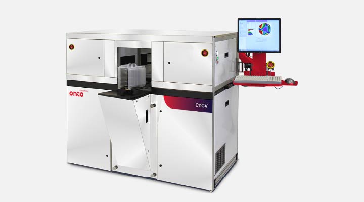
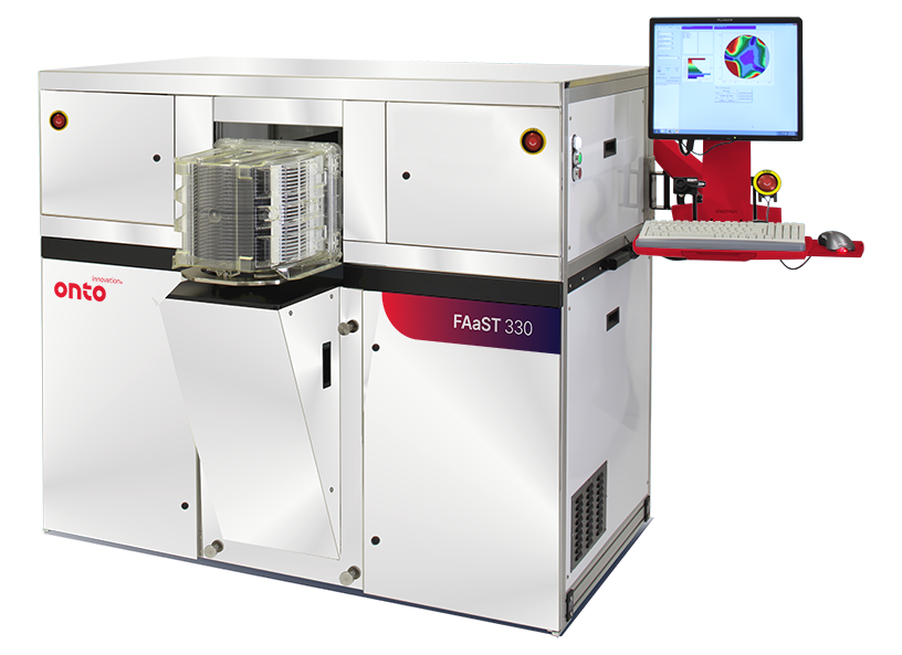
The FAaST system is a versatile, non-contact electrical metrology platform, with an option to combine micro and macro corona-Kelvin technologies together with digital surface photovoltage (SPV). It enables high-resolution dielectric and interface measurements across a wide range of dielectric materials, supporting both R&D and high volume manufacturing.
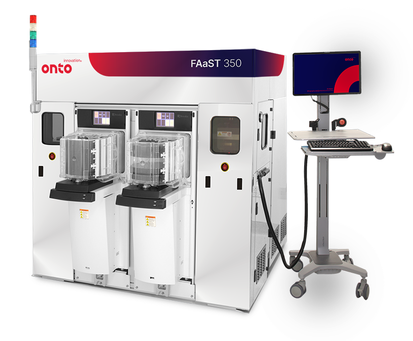
The primary application of non-contact CV metrology is monitoring dielectric properties during IC manufacturing. Unlike conventional electrical measurements, it requires no sample preparation, eliminating the need for MOS capacitor structures. This reduces metrology cost and enables fast data feedback in both R&D and manufacturing environments.
The corona-Kelvin method uses a corona discharge in air to deposit an electric charge (DQC) on the wafer surface. A vibrating Kelvin-probe then measures the resulting surface voltage (V), enabling determination of the differential capacitance (C= DQC/DV). By monitoring surface voltage in both dark and illuminated conditions, the system separates two key components: dielectric voltage (VD) and semiconductor surface potential (VSB), enabling determination of flat band voltage (VFB).
Analysis of the resulting charge-voltage data yields electrical parameters, including trap density (Dit), flat band voltage (Vfb), dielectric charge (Qtot), dielectric capacitance (CD), Equivalent Oxide Thickness (EOT), leakage current, and tunneling characteristics.
As your partner for innovative solutions, we’re always here for you.
Discover how our cutting-edge semiconductor solutions are engineered to meet your most complex challenges: delivering performance, reliability and innovation where it matters most.
"*" indicates required fields
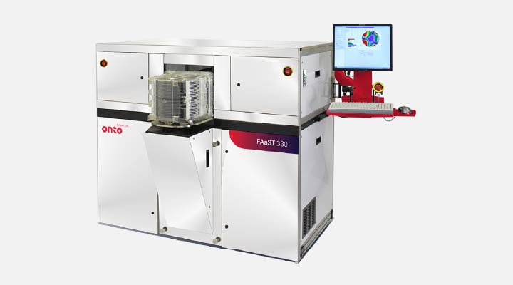
The Aspect S system is a revolutionary in-line, non-destructive model-based infrared reflectometry system that enables critical process control of high aspect ratio structures, films and epitaxial structures. It meets the needs of leading-edge customers with its high speed and process coverage.
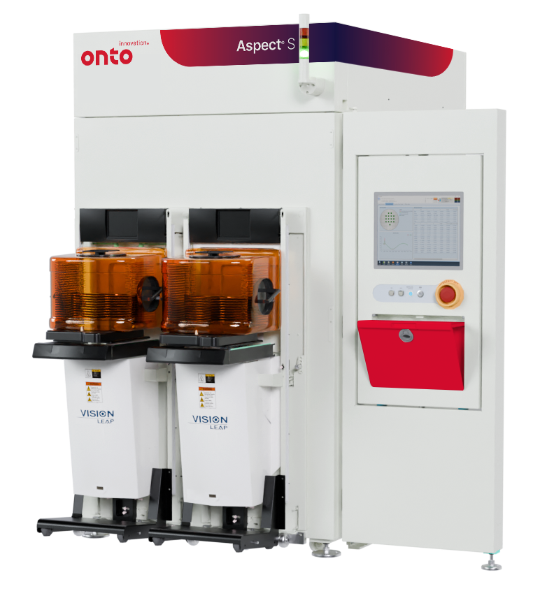
As more high aspect ratio processes are used in multiple industry segments, there are metrology needs for monitoring of related processes, including dimensions and properties of carbon film hard masks and etched 3D structures.
The Aspect S delivers high-throughput, low COO, non-contact, non-destructive measurements of dimensions and uniformity of layers and etched structures used in integrated circuit manufacturing. The small spot size makes the tool suitable for measurements of scribe line test structures as in-line process control. The unique technology and analysis capability simplifies system calibration requirements and removes the effect of substrate variations for key layer measurements.
While the software contains advanced features for measurement recipe and analysis model creation, it has a user-friendly interface and implementation that allows the fab customers to create and manage the recipe system for Aspect S tool fleets.

Thickness map from amorphous carbon film
As your partner for innovative solutions, we’re always here for you.
Discover how our cutting-edge semiconductor solutions are engineered to meet your most complex challenges: delivering performance, reliability and innovation where it matters most.
"*" indicates required fields
The FAaST Digital SPV system provides a fast, non-contact, and preparation-free method for full wafer imaging of contamination in silicon. High resolution maps of diffusion length and iron (Fe) concentration are generated in minutes, setting the industry standard for precision and sensitivity in Fe contamination control, reaching the E7 cm-3 range.
There is no disputing the detrimental effect of metallic contamination on the integrity of the critical gate oxide used in integrated circuits. During high temperature processing, contamination in the silicon wafer often precipitates at the Si/dielectric interface or segregates into the dielectric—both scenarios can cause premature device failure and reduced yield. As device dimensions shrink, the tolerance for contamination decreases, requiring ever-lower background levels of metals like iron (Fe). Over the past 25 years, the IC industry has reduced typical Fe concentrations by more than three orders of magnitude, yet further reduction is essential, especially for applications like CMOS image sensors.
The FAaST Digital SPV system addresses this challenge with industry-leading sensitivity and speed. It provides a fast, non-contact, and preparation-free method for full-wafer imaging of contamination. High-resolution maps of minority carrier diffusion length and Fe concentration are generated in minutes, enabling fabs to detect and control contamination at levels as low as the E7 cm⁻³ range.

Figure 1. Typical background Fe concentration in new IC Fablines (blue) and the state-of-the-art SPV detection limit (red)
As your partner for innovative solutions, we’re always here for you.
Discover how our cutting-edge semiconductor solutions are engineered to meet your most complex challenges: delivering performance, reliability and innovation where it matters most.
"*" indicates required fields