
Dragonfly® G3 System
Highly configurable, automated, high speed 2D inspection and 3D metrology for inline process control in advanced packaging, specialty and front-end OQA.

If you’ve been following the evolution of advanced packaging, you know that the industry is pushing boundaries like never before. From high-performance computing to industry-upending AI devices, the demand for smaller, faster, and more powerful chips is driving innovation at every level.

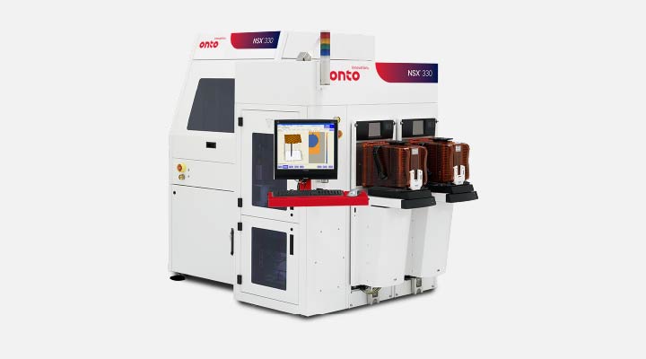
The NSX 330 system offers advanced macro inspection for a wide range of defect sizes at high throughput, with optional 3D metrology integration.
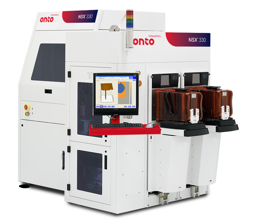
The NSX 330 system features robust platform technology with high-acceleration staging, high-speed multi-processor computing and flexible software. With over 1,000 installation worldwide, the NSX 330 System offers 2D inspection and metrology at high throughput and a broad portfolio of 3D sensors supporting critical advanced packaging applications. These include wafer-level metrology for micro bumps, RDL, kerf, overlay, and through silicon via (TSV) in a single wafer load.
Accommodating wafers from 100mm to 330mm, the system features a versatile objective turret, programmable light tower, and multiple dark field illumination modes. Additional features include resolution flexibility, unique handling solutions, and comprehensive software for recipe sharing and offline analysis. The NSX 330 system, with optional edge and backside inspection via the EB40 module, provides a comprehensive all-surface inspection solution packaging technology challenges.


As your partner for innovative solutions, we’re always here for you.
Discover how our cutting-edge semiconductor solutions are engineered to meet your most complex challenges: delivering performance, reliability and innovation where it matters most.
"*" indicates required fields
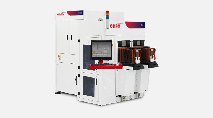
The F30 system is designed to blur the lines between dark field micro inspection and traditional macro inspection, providing automated defect inspection for front-end and outgoing quality (OQA) applications.
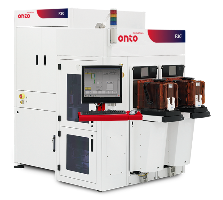
The F30 automated defect inspection system combines high resolution and throughput to drive fab yield and productivity. A five-objective turret enables resolution-throughput flexibility, while its multi-channel illumination including brightfield, darkfield, high-angle ring light, and IR-Review addresses the requirements for today’s multi-process inspection applications. Equipped with an advanced productivity suite (waferless recipe creation, simultaneous FOUP, recipe server and tool matching), the F30 System redefines inspection cost of ownership expectations. The system can handle 100mm – 300mm wafers can be paired with the edge and backside module (EB40) to provide an all-surface inspection solution.

As your partner for innovative solutions, we’re always here for you.
Discover how our cutting-edge semiconductor solutions are engineered to meet your most complex challenges: delivering performance, reliability and innovation where it matters most.
"*" indicates required fields
The Celero PL system is designed for subsurface defect inspection and classification for silicon carbide (SiC) and gallium nitride (GaN) based wafers and compound semiconductor materials.
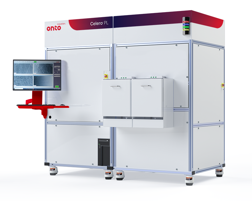
The Celero PL system utilizes a laser-based phase detection and imaging capability that leverages custom optics and image processing algorithms to enable best in class throughput and sensitivity for silicon carbide and gallium nitride-based materials on 100mm to 300mm wafer sizes. Leveraging multiple light sources and sensor channels, the system can detect, measure and image a broad variety of subsurface crystalline defects, associated with bulk wafers and epitaxial layers, surface particles, scratches, pits, surface contamination, stains, point or bulk wafer stress, voids/inclusions, including chips and cracks at the edge of the wafer.


As your partner for innovative solutions, we’re always here for you.
Discover how our cutting-edge semiconductor solutions are engineered to meet your most complex challenges: delivering performance, reliability and innovation where it matters most.
"*" indicates required fields
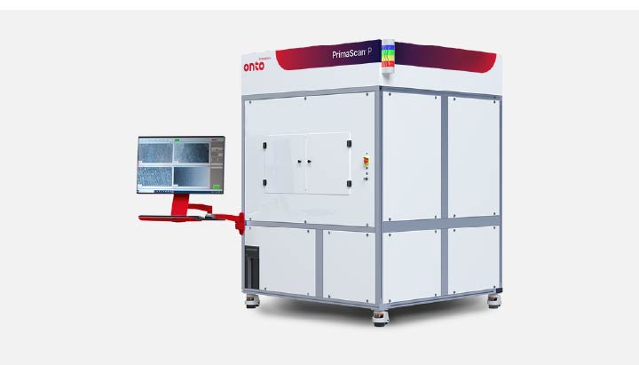
The PrimaScan P System provides all-surface defect and contamination inspection with imaging capability for glass panel substrates.
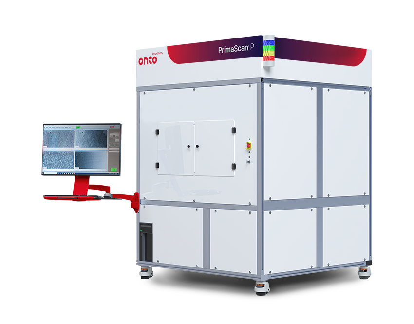
As panel-level-packaging (PLP) transition from copper-clad laminates (CCL) to glass, the industry must adapt to ensure starting substrates are free of killer defects and contamination or latent defects that may result in yield loss or scrapped panels at later stages in the process flow. The PrimaScan P system is specifically designed to address incoming glass panel quality control for both the advanced IC substrate (AICS) and fan-out panel level processing (FOPLP) segments.
The PrimaScan P system delivers unique laser-based scanning and imaging via proprietary optics and sensing technologies for the reliable inspection of nanometer sized defects for either R&D or high-volume manufacturing environments. Utilizing multiple channel inspection technologies, the system can detect, measure and image surface particles, scratches, pits, surface contamination, stains, film or bulk panel stress, voids/inclusions, including chips and cracks at the edge of the panel.
As your partner for innovative solutions, we’re always here for you.
Discover how our cutting-edge semiconductor solutions are engineered to meet your most complex challenges: delivering performance, reliability and innovation where it matters most.
"*" indicates required fields
The PrimaScan R&D System is a stand-alone, manual load version of the PrimaScan automated wafer defect and contamination inspection system that has been specifically designed with R&D and lab environments in mind.
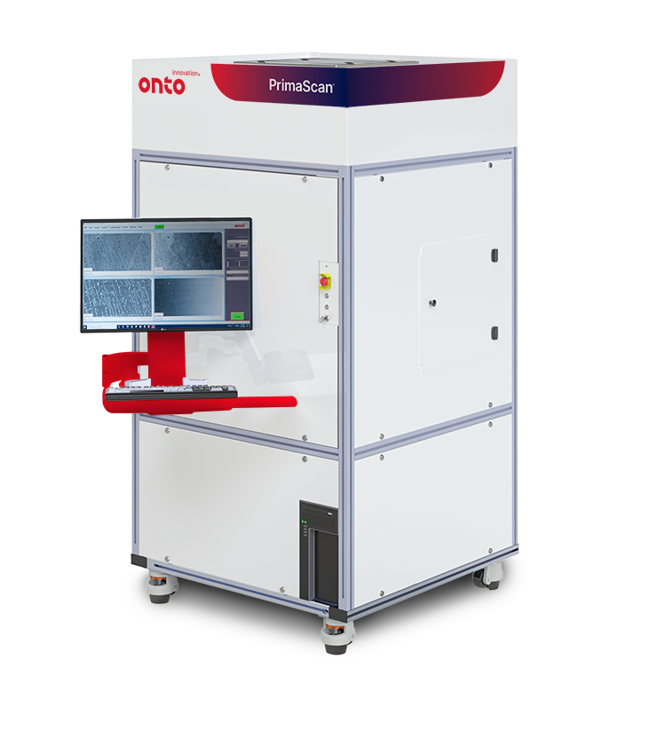
The PrimaScan R&D system offers a smaller spot size and higher pixel resolution than its high volume production counterpart tools. The flexibility in sample handling options combined with the multiple sensing channels and higher resolution imaging makes this the ideal tool for R&D and lab environments. Similar to the other tools in the PrimaScan line, the PrimaScan R&D system offers reliable inspection of nanometer sized defects on a variety of opaque and transparent/semi-transparent substrates and samples suitable for either R&D or lab environments. The system can detect, measure, characterize and image surface particles, scratches, pits, bumps, surface contamination, film or bulk wafer stress, voids/inclusions, including chips and cracks at the wafer edge.
Designed with versatility in mind the PrimaScan R&D system can handle a variety of wafer sizes and substrate types including film frame, photomask and sample tray.
As your partner for innovative solutions, we’re always here for you.
Discover how our cutting-edge semiconductor solutions are engineered to meet your most complex challenges: delivering performance, reliability and innovation where it matters most.
"*" indicates required fields
The EB40 Module combines edge and backside inspection into one tool with the option to be paired with an inspection system to provide a high throughput all surface inspection solution.
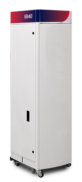
The Class 1 certified EB40 module offers combined edge and backside inspection and is also available as separate edge (E40) and backside (B40) modules. These modules provide brightfield and darkfield inspection to detect defects on the entire bevel and backside, covering Zone 1 to Zone 5. This enables faster root-cause analysis of defects that can migrate to the wafer interior, impacting die yield.
The EB40 module captures defect images on the fly, creates whole-wafer composite images, and integrates with SEM bevel review. All inspection and metrology results, including defect, whole wafer and SEM images can be analyzed together in a single database using Discover Defect software. Correlating EBR metrology with defectivity data, SEM data and micro-inspection results is just the beginning of what Discover software can do. In addition to advanced on-tool defect binning, real-time edge ADC classification can be assigned to defects prior to manual offline review using Discover Review software.


As your partner for innovative solutions, we’re always here for you.
Discover how our cutting-edge semiconductor solutions are engineered to meet your most complex challenges: delivering performance, reliability and innovation where it matters most.
"*" indicates required fields