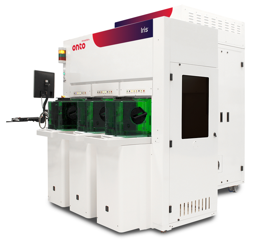
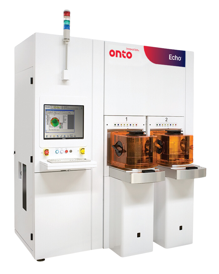
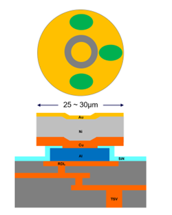
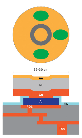
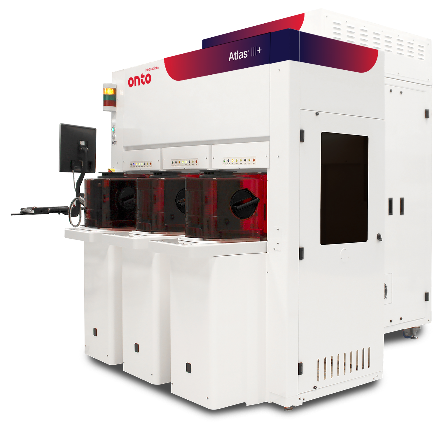
The Iris S system delivers films metrology and advanced OCD capabilities for the specialty and advanced packaging segments. With a small footprint, it handles 150mm, 200mm, and 300mm wafer sizes, including thin, thick and bonded wafers. The system supports various materials such as Si, SiC, GaN and glass, addressing device-level challenges impacting performance and yield. Leveraging Onto’s Ai Diffract™ software, the Iris S system supports the most difficult on-wafer high value problems.
The Iris S system includes a dual-arm robot, high-precision stage, advanced pattern recognition, and high-speed focus for accurate positioning at high throughput. The dual channel optical architecture offers oblique incidence Mueller Matrix spectroscopic ellipsometry (MMSE) and normal incidence spectroscopic reflectometry (SR) in a broad wavelength range from UV to IR.
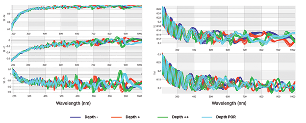
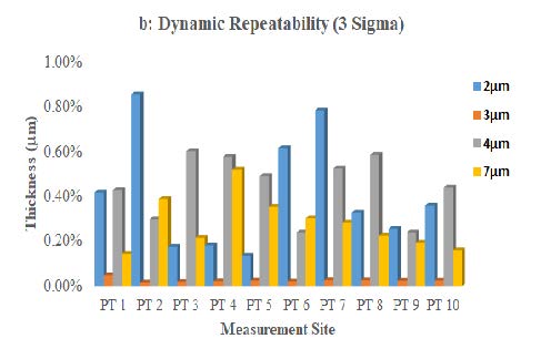
Based on Windows 10 OS and a 64-bit architecture, the Ai Diffract™ software interface and automation comply with SEMI standards. Onto’s model guided machine learning enables fast, flexible and robust film and OCD recipe setup.