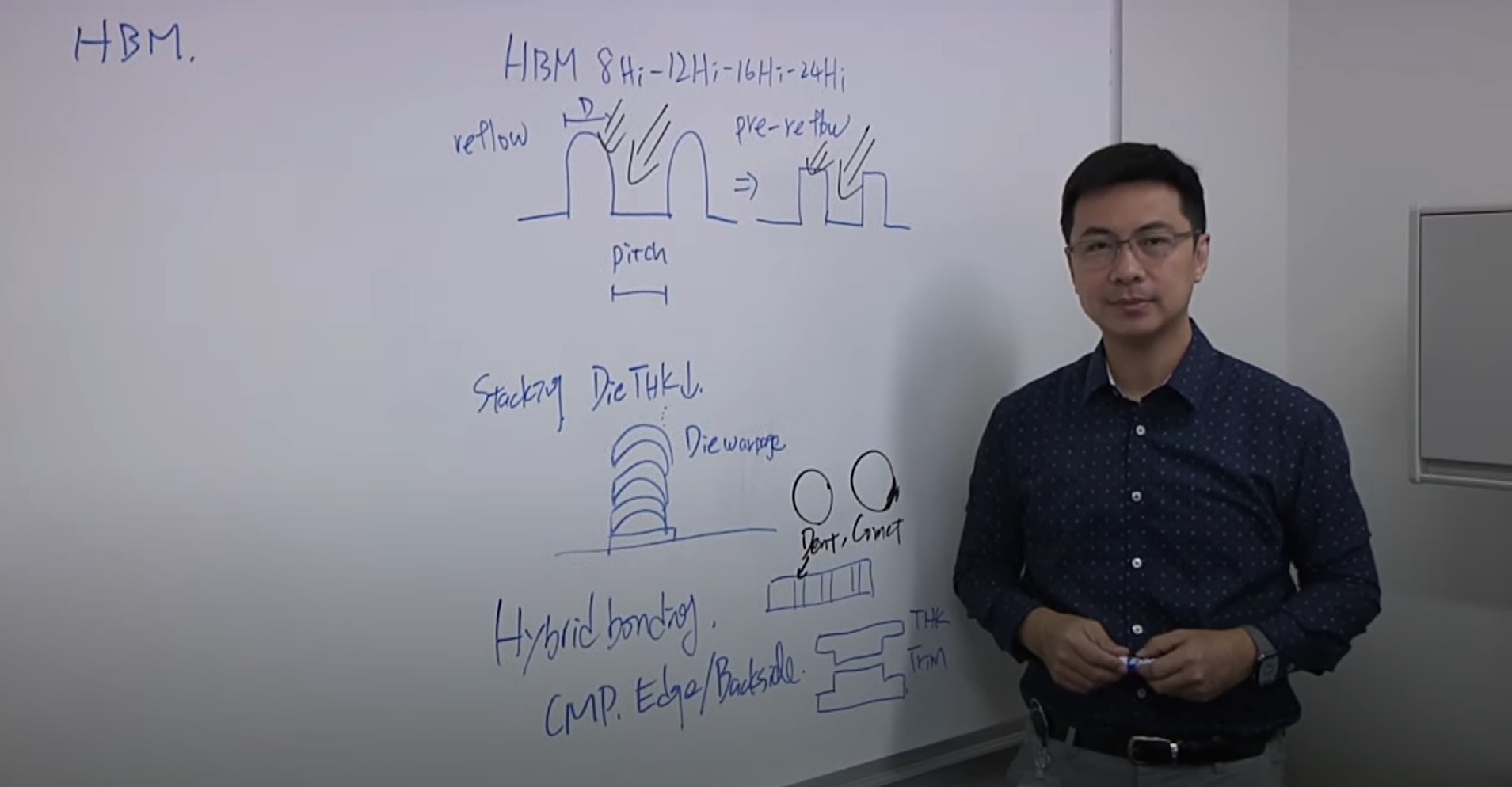

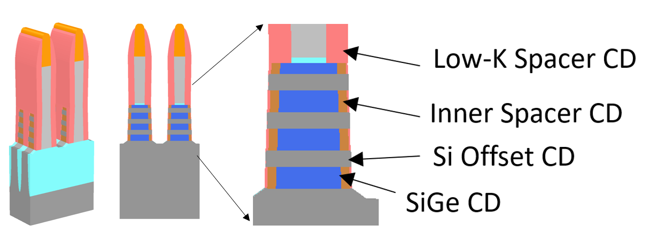
Optical Critical Dimension Metrology for Semiconductor Manufacturing
Vacuum based processes are essential in the semiconductor manufacturing process. In the simplest terms, integrated circuits are composite structures fabricated one layer at a time. Each layer is deposited as a blanket film, then patterned by removing material in selected areas. The final, three-dimensional structure, made up of insulating, conducting, and semiconducting components, forms a functional circuit. Most of the deposition and removal steps take place in a vacuum environment, which creates the physical conditions required for the process to proceed, ensures the purity of the material deposited, and removes excess process chemicals and by-products from the process chamber. Throughout its history, the semiconductor industry has defined progress almost exclusively by its ability to reduce the size of the devices it creates. Measuring critical dimensions of the component structures and controlling the manufacturing process to ensure high yields of functional devices have been a critical requirement for progress. These structures became too small to resolve with image based light microscopy decades ago. Manufacturers now rely on scatterometry for optical critical dimension (OCD) measurements. Because it is not image based, scatterometry is not constrained by the diffraction effects that limit image resolution. Furthermore, and especially important for current device architectures, scatterometry can provide three-dimensional measurements. In this article we will look at the fundamentals of OCD and provide some examples of its use on simple, representative structures.