Addressing Copper Clad Laminate Processing Distortion Using Overlay Corrections

All great voyages must come to an end. Such is the case with our series on the challenges facing the manufacturing of advanced IC substrates (AICS), the glue holding the heterogeneous integration ship together.
In our first blog, we examined how cumulative overlay drift from individual redistribution layers could significantly increase overall trace length, resulting in higher interconnect resistance, parasitic effects and poor performance for high-speed and high-frequency applications. To address this, layer to layer overlay performance data needs to be monitored at each layer. If the total overlay error exceeds specifications at any process step, and at any location on the panel, corrective action must be taken to mitigate the drift in total overlay.
For this second installment, we explored the issue of AICS package yield and its importance in fostering a cost-effective, production-worthy process. Unlike most fan-out panel-level packaging (FOPLP) applications, AICS has relatively few packages per panel. This enormous disparity impacts yield calculations dramatically. In the AICS production process, the main challenge is the real-time tracking of yield for every panel, at every layer, throughout the fab. The solution: using advanced automatic defect classification (ADC) and yield analytics to quickly address errors.
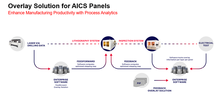
In this final article of the series, we explore how overlay correction solutions compensate for panel distortion effects induced by copper clad laminate (CCL) processing, which impacts yield and final package performance.

