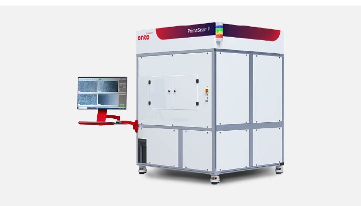
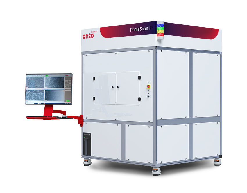
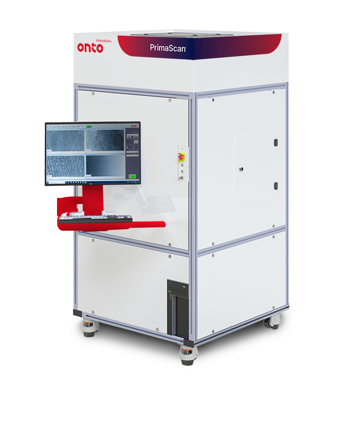
PrimaScan™ P System
All-surface defect and contamination inspection for unpatterned glass panel substrates with imaging capability for panels up to 600x600mm in size.
In a world where high-bandwidth memory, GPUs, and advanced AI packages are all the rage, it is easy to forget the important role specialty devices play.

May 5 — May 7, 2026
Onto Innovation is a proud exhibitor at SEMICON Southeast Asia.
The PrimaScan wafer defect inspection system delivers a flexible, high sensitivity solution at the lowest cost of ownership per pass.
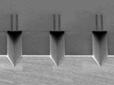
The PrimaScan system utilizes laser scatterometry and imaging techniques leveraging proprietary optics and sensing technologies for reliable inspection of nanometer sized defects on a variety of opaque and transparent/semi-transparent substrates suitable for either R&D or high-volume manufacturing environments. With multiple detection channels, the system can detect, measure, characterize and image surface particles, scratches, pits, bumps, surface contamination, film or bulk wafer stress, voids/inclusions, including chips and cracks at the wafer edge.
The PrimaScan system addresses challenges in both incoming wafer quality control and in inline process monitoring. Capable of handling multiple substrate materials, it uniquely addresses inline process defect and contamination monitoring in wafer-based production environments.
Designed with versatility in mind the PrimaScan system can handle a variety of wafer sizes and substrate types


As your partner for innovative solutions, we’re always here for you.
Discover how our cutting-edge semiconductor solutions are engineered to meet your most complex challenges: delivering performance, reliability and innovation where it matters most.
"*" indicates required fields
The PrimaScan P System provides all-surface defect and contamination inspection with imaging capability for glass panel substrates.
As panel-level-packaging (PLP) transition from copper-clad laminates (CCL) to glass, the industry must adapt to ensure starting substrates are free of killer defects and contamination or latent defects that may result in yield loss or scrapped panels at later stages in the process flow. The PrimaScan P system is specifically designed to address incoming glass panel quality control for both the advanced IC substrate (AICS) and fan-out panel level processing (FOPLP) segments.
The PrimaScan P system delivers unique laser-based scanning and imaging via proprietary optics and sensing technologies for the reliable inspection of nanometer sized defects for either R&D or high-volume manufacturing environments. Utilizing multiple channel inspection technologies, the system can detect, measure and image surface particles, scratches, pits, surface contamination, stains, film or bulk panel stress, voids/inclusions, including chips and cracks at the edge of the panel.

As your partner for innovative solutions, we’re always here for you.
Discover how our cutting-edge semiconductor solutions are engineered to meet your most complex challenges: delivering performance, reliability and innovation where it matters most.
"*" indicates required fields
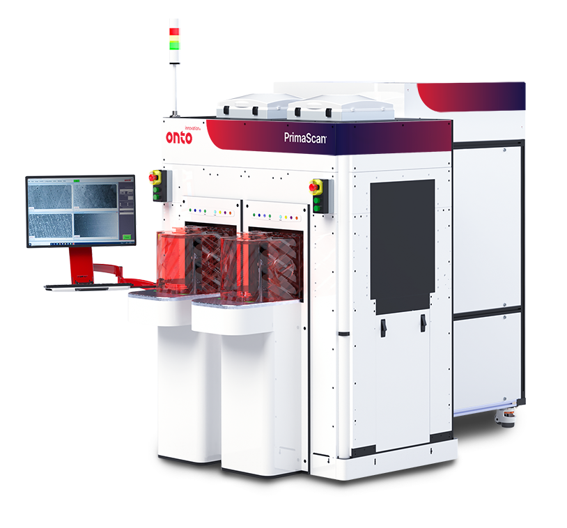
The PrimaScan R&D System is a stand-alone, manual load version of the PrimaScan automated wafer defect and contamination inspection system that has been specifically designed with R&D and lab environments in mind.
The PrimaScan R&D system offers a smaller spot size and higher pixel resolution than its high volume production counterpart tools. The flexibility in sample handling options combined with the multiple sensing channels and higher resolution imaging makes this the ideal tool for R&D and lab environments. Similar to the other tools in the PrimaScan line, the PrimaScan R&D system offers reliable inspection of nanometer sized defects on a variety of opaque and transparent/semi-transparent substrates and samples suitable for either R&D or lab environments. The system can detect, measure, characterize and image surface particles, scratches, pits, bumps, surface contamination, film or bulk wafer stress, voids/inclusions, including chips and cracks at the wafer edge.
Designed with versatility in mind the PrimaScan R&D system can handle a variety of wafer sizes and substrate types including film frame, photomask and sample tray.
As your partner for innovative solutions, we’re always here for you.
Discover how our cutting-edge semiconductor solutions are engineered to meet your most complex challenges: delivering performance, reliability and innovation where it matters most.
"*" indicates required fields