

Abstract
As advanced packaging architectures continue to scale in complexity, the role of die and bump inspection has become increasingly critical for ensuring yield, reliability, and process control in both wafer‑level and panel‑level manufacturing environments. The transition toward heterogeneous integration, chiplet‑based designs, and fine‑pitch interconnects places unprecedented demands on metrology systems responsible for validating die quality, bump integrity, and overall assembly readiness.
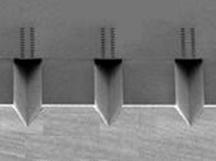
Fine‑pitch microbumps, copper pillars, and hybrid bonding interfaces now routinely require dimensional tolerances at sub‑micron levels. Variations in bump height, coplanarity, diameter, oxidation, and surface morphology can significantly impact downstream bonding performance, electrical continuity, and thermal integrity. As interconnect densities approach tens of thousands of bumps per die, even low‑level defectivity—such as voids, non‑wet bumps, foreign material, or micro‑cracks—becomes yield‑limiting. Consequently, high‑resolution optical inspection, advanced 3D metrology, and machine‑learning‑driven defect classification are essential to differentiate critical defects from benign process variations.
At the panel level, larger form factors introduce additional challenges: increased warpage, non‑uniform process distributions, and the need for wide‑field, high‑throughput inspection without sacrificing sensitivity. These constraints drive demand for scalable metrology architectures capable of combining large‑area imaging with precise local 3D measurements. The ability to track die placement accuracy, pillar geometry, and redistribution layer (RDL) alignment is fundamental to ensuring consistent performance across large substrates.
Overall, advanced die and bump inspection technologies have become indispensable for enabling high‑yield, high‑reliability packaging processes. As feature sizes shrink and integration complexity rises, these metrology capabilities form the foundation for robust assembly across next‑generation wafer‑ and panel‑level platforms.
This presentation highlights the most critical of these challenges today and provides examples of where the latest technologies in 3D laser based metrology and high speed infra-red defect inspection can be applied to mitigate the effects of such defects in production, ensuring high yield wafer and/or panel level products.
Event Details
Event: ISIG Executive Summit Taiwan| Date | May 13, 2026 |
|---|---|
| Time | 9:40 a.m. — 10:00 a.m. |
| Location | Taipei, Taiwan |
| Event | ISIG Executive Summit Taiwan |
| Presenters |