

CMOS Technologies
As CMOS technologies become more complex, device manufacturers require more advanced process control products to identify critical and killer defects, and to monitor critical dimensions, films, and material properties of bulk wafers, layers and critical films.
Today, Complementary Metal Oxide Semiconductor (CMOS) technologies range in complexity from the most advanced 2nm Gate-all-Around (GAA) logic devices to the tallest 3D NAND stack, or highest bit density DRAM device technologies. For each, Onto Innovation supports customers with advanced optical critical dimension (OCD) technologies that enable a variety of highly accurate measurements critical to device performance and yield. Whether integrated on partner OEM tools or standalone, our OCD or films metrology portfolio of products are widely used and continue to be adopted to solve some of the industry’s most difficult high value problems.
Advanced Logic Devices
The most advanced logic devices at 7nm or below include FinFet, GAA or CFET technologies. Each specialized device architecture requires extreme critical dimension metrology delivered at high volume manufacturing (HVM) throughputs. In addition, the unique structures of these devices also requires both materials analysis and precise film thickness metrology.


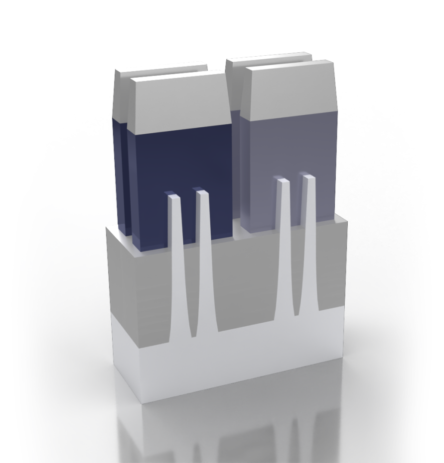
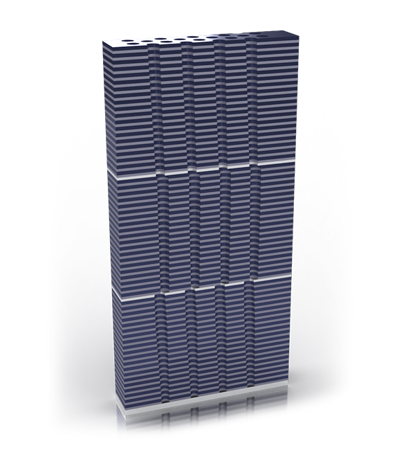
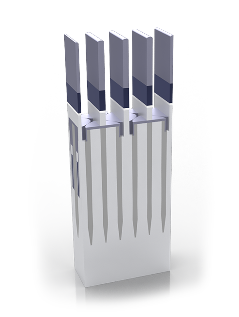
3D NAND
3D NAND memory requires cells to be stacked vertically, increasing storage density and performance. Today’s 3D NAND memory architectures increase bit density by continuously pushing the limits of stacked process layers. Extending beyond >500 layers, alternating O-N-O-N layer pairs are interconnected by a high aspect ratio trench filled with metal. This extreme etch requires precise CD and profile metrology as well as films thickness metrology. Onto Innovation delivers a unique set of IR and mid-IR OCD and single wavelength films metrology tools designed specifically to meet the challenges of this rapidly evolving device segment.
DRAM
Modern Dynamic Random Access Memory (DRAM) faces numerous scaling challenges from bit density to device stacking to 3D integration of materials. Onto Innovation utilizes multiple technologies within its advanced OCD and films metrology portfolio as well as its high-resolution front-end wafer inspection product offerings to support the latest DDR or high bandwidth memory (HBM) DRAM memory technologies.

Do you have a CMOS technology question? Let’s talk!
As your partner for innovative solutions, we’re always here for you.
Discover how our cutting-edge semiconductor solutions are engineered to meet your most complex challenges: delivering performance, reliability and innovation where it matters most.
Let’s Talk
"*" indicates required fields