Bare Wafer & Panel Level Manufacturing
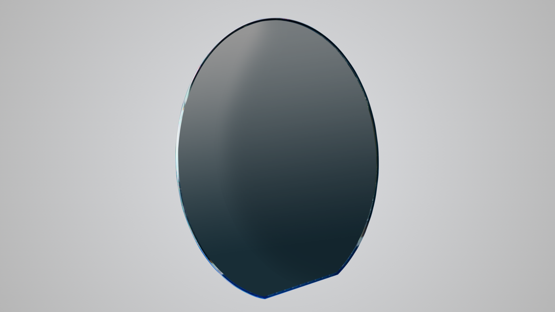
Bare and unpatterned substrates serve multiple applications from advanced logic and memory to specialty and mature semiconductor devices, including both wafer and panel level substrates used in advanced packaging.
Efficient semiconductor production and manufacturing processes begin with quality control of incoming bare and unpatterned substrates. These substrates, whether bare silicon, silicon with epitaxial layers, or bare glass panels, are essential for various applications. Suppliers are constantly striving to improve process capability and reduce production costs by controlling critical wafer characteristics. These include impurities in silicon, epitaxial thickness and variation, edge and notch defect monitoring, tighter edge exclusion zones, bulk and epitaxial resistivity, surface defects and contamination and subsurface inclusions or micro cracks in glass panels.


Do you have a bare wafer or panel manufacturing question? Let’s talk!
As your partner for innovative solutions, we’re always here for you.
Discover how our cutting-edge semiconductor solutions are engineered to meet your most complex challenges: delivering performance, reliability and innovation where it matters most.
Let’s Talk
"*" indicates required fields

