

Advanced Packaging
Advanced packaging includes both wafer level packaging (WLP) and panel level packaging (PLP) application segments. Onto Innovation offers a comprehensive range of product solutions for advanced packaging, including lithography, metrology and inspection-based products.
The advanced packaging segment in the semiconductor industry is experiencing rapid growth and innovation, driven by the increasing demand for high-performance devices comprising a mixture of device architectures and technologies. Advanced packaging techniques, such as flip chip, embedded die, fan-in wafer-level packaging (FI-WLP), fan-out wafer-level packaging (FO-WLP), and 2.5D/3D integration, are revolutionizing how chips are assembled and interconnected. Today, these integration techniques are further expanded upon with the introduction of advanced panel level processing (PLP). Panel level processing takes the advanced packaging mindset further down the device integration path by enabling the integration of multiple individual or stacked devices on a panel substrate. This substrate can be made from either copper clad laminate (CCL) or glass. The nature of the panel material along with the number of redistribution layers needed, dictate the relative complexity of the panel fabrication and ensuing die level integration process. Overall, these integration methods enhance the performance, functionality and reliability of semiconductor devices by enabling higher transistor densities, improved thermal management and faster data transfer rates.
Onto Innovation’s unique portfolio of products support the advanced packaging market in both WLP and PLP segments, by providing lithography, inspection and metrology products to address the most difficult and high value problems facing the industry today.
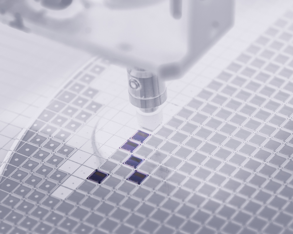
Wafer Level Packaging (WLP)
Wafer level packaging (WLP) is an advanced semiconductor packaging technology where integrated circuits are packaged directly at the wafer level, rather than after individual dies are separated. This method streamlines the manufacturing process, enhancing efficiency and reducing costs. WLP involves adding protective layers and electrical connections to the entire wafer before dicing it into individual chips. This approach results in smaller, thinner and more efficient devices, making it ideal for applications requiring compact and high-performance components, such as mobile devices and wearables. Onto Innovation’s product portfolio of metrology and inspection tools provides customers with unique technologies designed to improve yield and productivity at both the wafer level or die level integration steps for WLP.


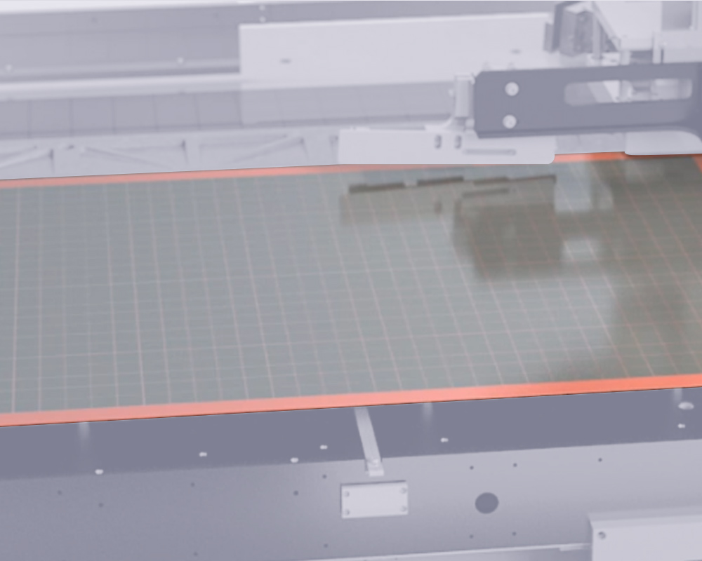
Panel Level Packaging (PLP)
Panel level packaging (PLP) is an advanced semiconductor packaging technique that shifts from the traditional wafer format to larger rectangular panels. This approach enhances manufacturing efficiency and reduces costs by enabling high volume production. PLP allows for the integration of multiple components onto a single panel, improving performance and functionality. It also supports heterogeneous integration, combining different types of chips and technologies within one package. As demand for miniaturized and high-performance electronic devices grows, PLP is becoming increasingly important in the semiconductor industry. Onto Innovation supports PLP with its portfolio of panel level lithography, inspection and metrology tools and software capabilities, assisting customers working with coper clad laminates (CCL) or glass substrates at a variety of line/space dimensions and field sizes.

Do you have an advanced packaging question? Let’s talk!
As your partner for innovative solutions, we’re always here for you.
Discover how our cutting-edge semiconductor solutions are engineered to meet your most complex challenges: delivering performance, reliability and innovation where it matters most.
Let’s Talk
"*" indicates required fields