

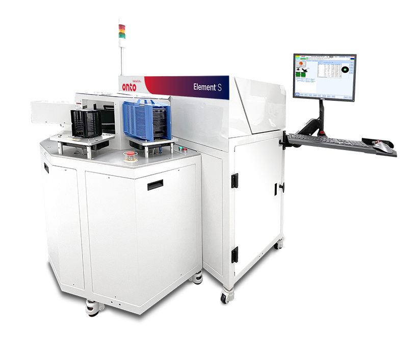
Element™ S System
The Element S system offers a unique combination of transmission and reflection-based technology, making it a valuable tool for dielectric monitoring.
Product Overview
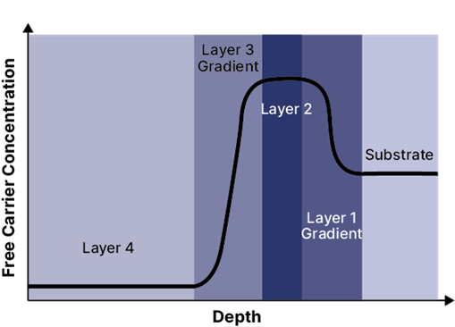
The Element S system is designed for the specialty market, specifically the smaller 100mm to 200mm wafer sizes used in the rapidly growing Si/SiC/GaN power device market. Building on the success of the Element Fourier transform infrared (FTIR) system, the Element S system can accurately measure thickness and free carrier concentrations in epitaxial layers up to five layers. This capability is essential for characterizing the thick epitaxial films required for next generation SiC power devices, which need thick epi layers for higher standoff voltage.
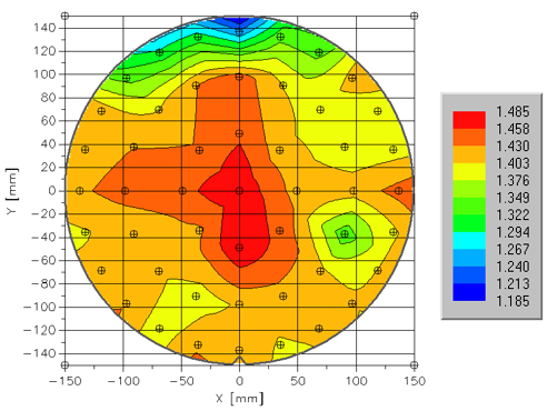
With its small spot size, the Element S system can conduct measurements up to the very edge of the wafer, maximizing die yield and enhancing productivity as power device customers transition to 200mm wafers. With improved sensitivity, an advanced multi-layer epi algorithm, and leading-edge multiple IR peak modeling, the Element S system provides critical and versatile capabilities for wafer and device makers in epi and film composition monitoring.
Applications
- Multi layer Epi layer, transition zone thickness and substrate concentration
- Power device EPI and buffer layer
- BPSG, FSG, SiN, HSQ, SiON, SiCN, SiOC
- Multiple IR peak metrics
- Interstitial oxygen and substitutional carbon
- Oxygen dose and Oxygen precipitate
Featured Markets
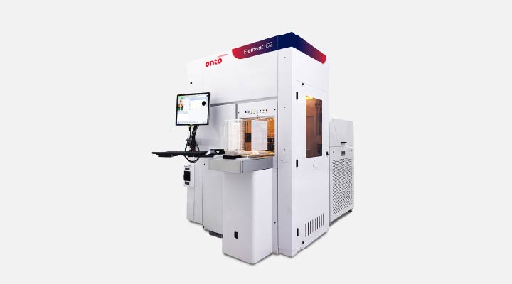
Element™ G2 System
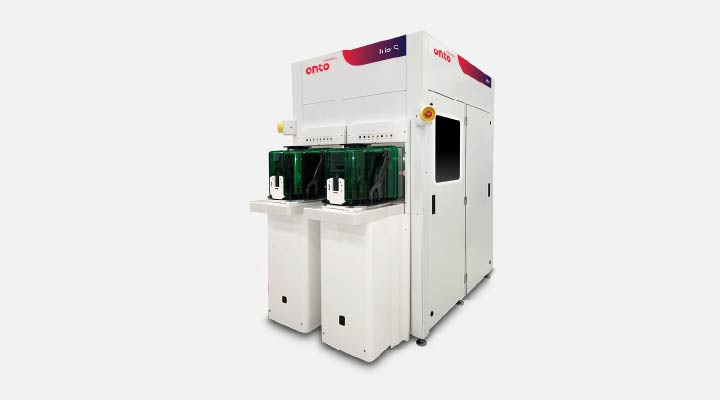
Iris™ S System
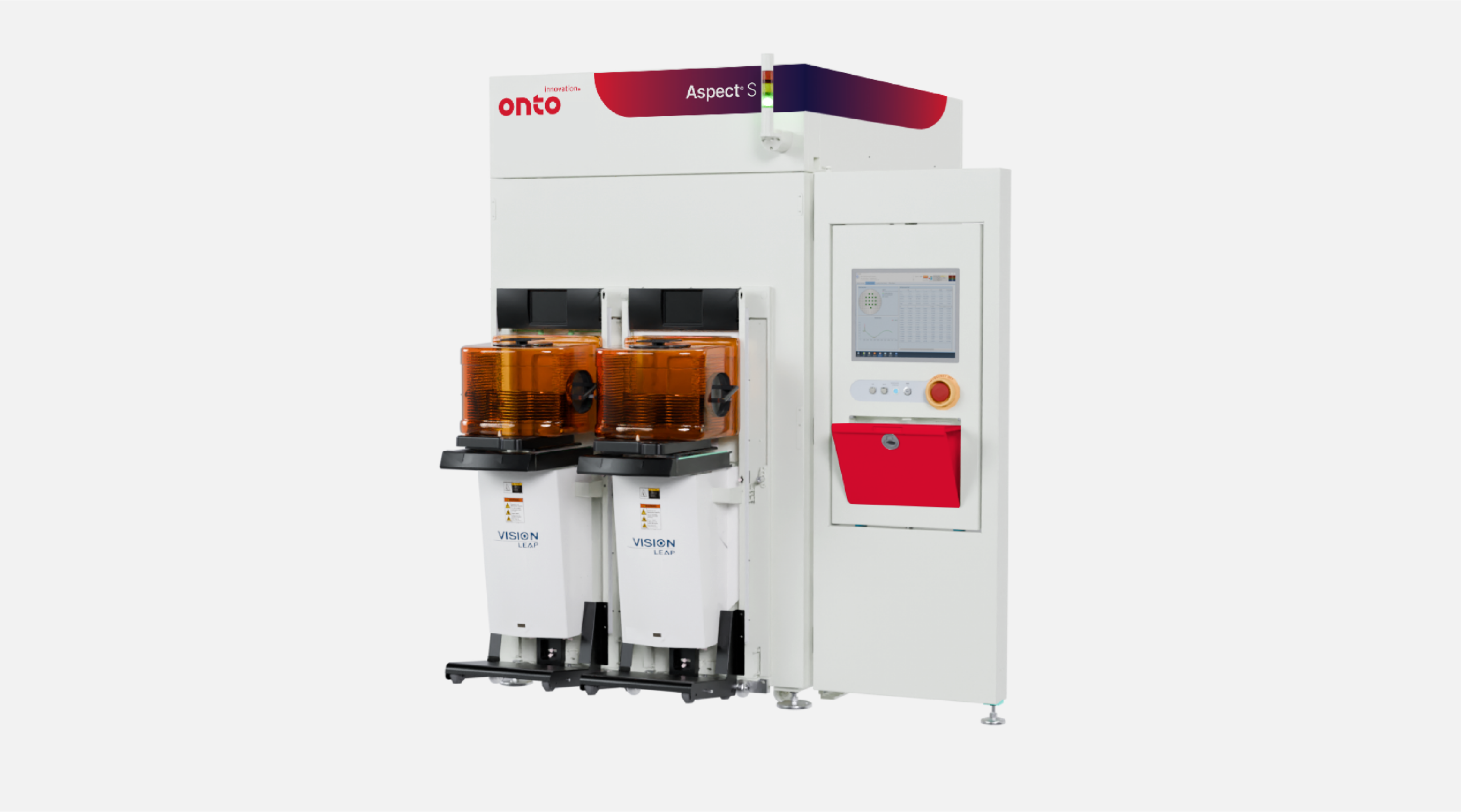
Aspect S System
Using FTIR To Improve SiC Power Device Performance

The Road to SiC Process Control
A Star is Born: Gallium nitride and the coming age of compound semiconductors
Advanced Modeling In FTIR Offers New Applications For HVM

Do you have an Element S system question? Let’s talk!
As your partner for innovative solutions, we’re always here for you.
Discover how our cutting-edge semiconductor solutions are engineered to meet your most complex challenges: delivering performance, reliability and innovation where it matters most.
Let’s Talk
"*" indicates required fields