

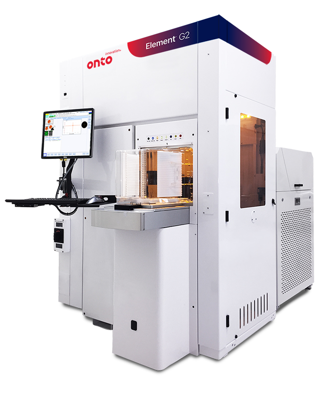
Element™ G2 System
The Element G2 system is a high-speed epitaxial layer metrology and wafer/film composition control system for wafer makers, advanced logic, DRAM and 3D NAND.
Product Overview
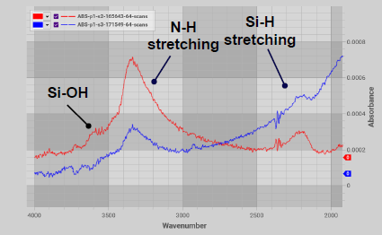
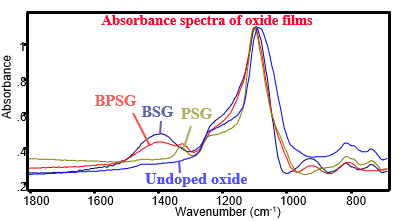
The Element G2 system is designed for wafer suppliers to perform high speed impurity mapping and epi thickness measurements. It combines transmission and reflection-based technology and when paired with advanced IR modeling capability, it offers a unique approach to dielectric composition and film thickness monitoring. With improved sensitivity and cutting-edge algorithms, the Element G2 system is a critical metrology tool widely used for monitoring dielectrics such as BPSG, FSG, H in SiN, and more. Machine learning helps eliminate the need for monitor wafers in dielectric measurement.
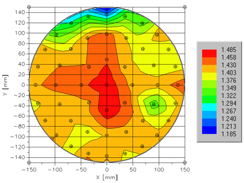
The system features a crisp 2mm circular IR spot, a high sensitivity interferometer and advanced pattern recognition. Equipped with a Class 1, five-axis dual-arm edge grip wafer handling system, the Element G2 system delivers high precision and high throughput, even at the edge of the wafer.
Applications
- Multi layer Epi layer, transition zone thickness and substrate concentration
- Power device EPI and buffer layer
- BPSG, FSG, SiN, HSQ, SiON, SiCN, SiOC
- Multiple IR peak metrics
- Interstitial oxygen and substitutional carbon
- Oxygen dose and Oxygen precipitate
Featured Markets
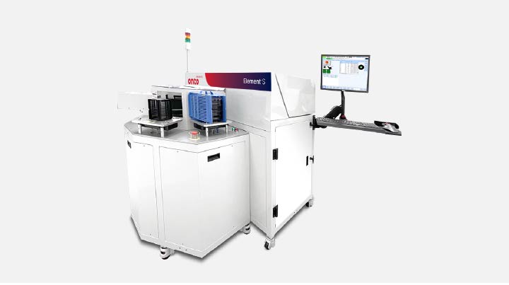
Element™ S System
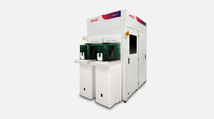
Iris™ S System
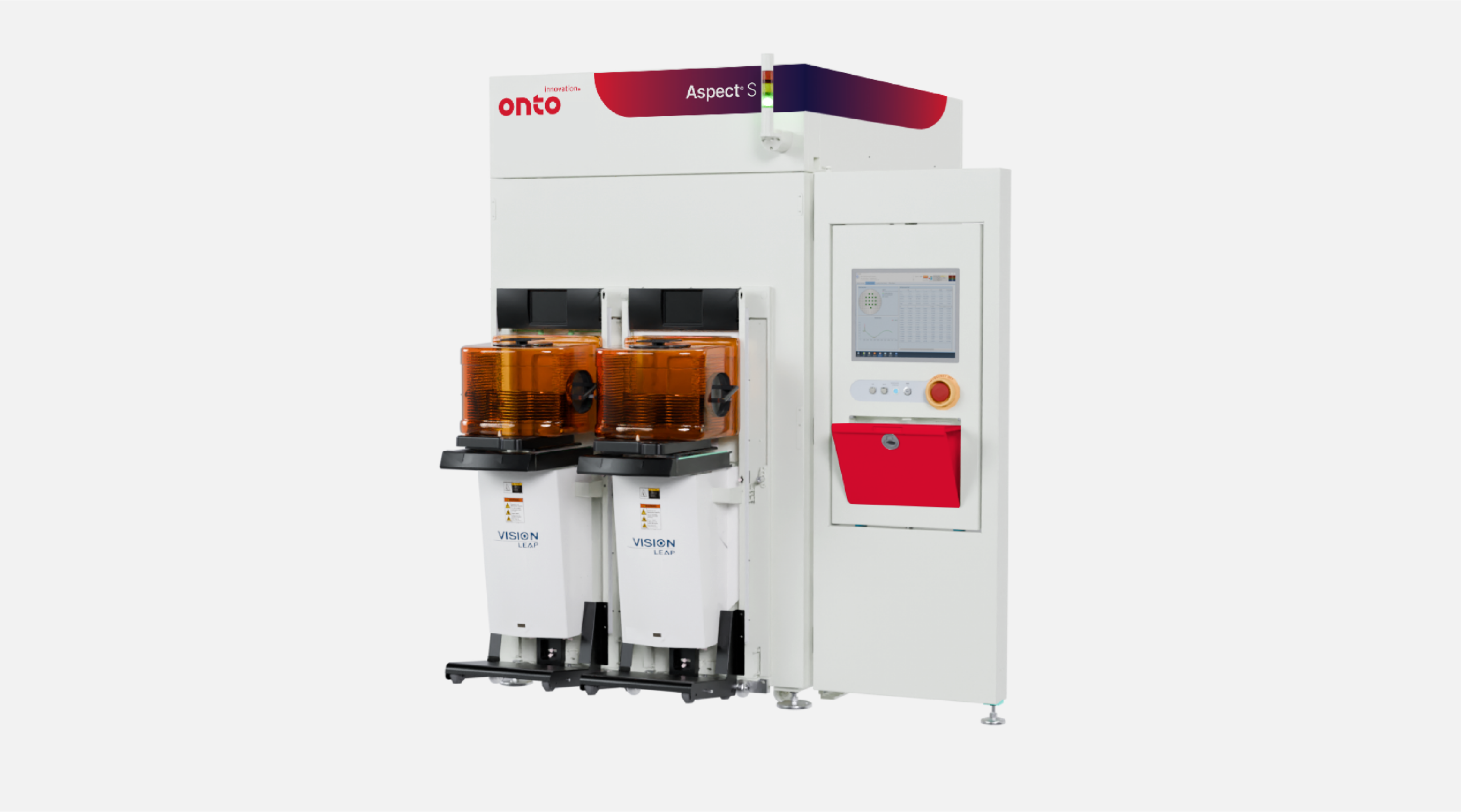
Aspect S System
Advanced FTIR Optical Modeling for Hydrogen Content Measurements in 3D NAND Cell Nitride and Amorphous Carbon Hard Mask
Advanced Modeling In FTIR Offers New Applications For HVM
Expanded Material Metrology For Refined Etch Selectivities

Do you have an Element G2 question? Let’s talk!
As your partner for innovative solutions, we’re always here for you.
Discover how our cutting-edge semiconductor solutions are engineered to meet your most complex challenges: delivering performance, reliability and innovation where it matters most.
Let’s Talk
"*" indicates required fields