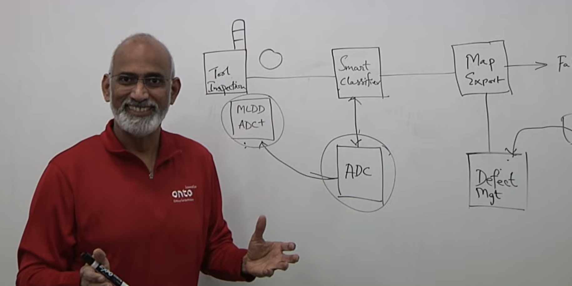

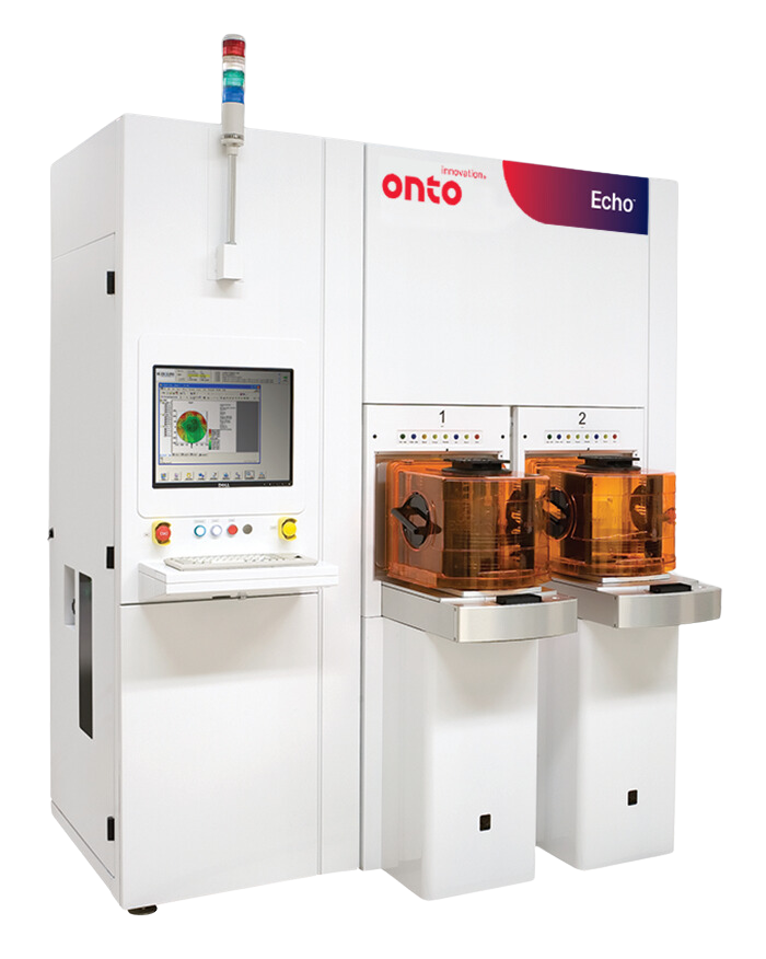
Echo™ System
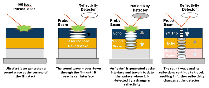
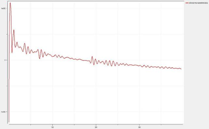
The Echo system utilizes picosecond ultrasonics to provide accurate, in-line, on-product metrology and materials characterization for semiconductor processes requiring metal thickness metrology, implant monitoring or thermal conductivity characterization on product wafers.
Product Overview
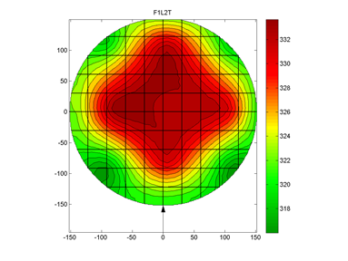
The Echo system is a comprehensive in-line metal film metrology tool designed for single and multi-layer metal film measurements in leading-edge logic, memory, advanced packaging and specialty semiconductor devices. Its innovative optics design extends the dynamic range for film thickness measurement from 50Å to 35µm on a single platform and offers extendibility to measure high aspect ratio advanced 3D NAND structures. The Expert Applications System (EASy™) software provides flexibility for developing user-defined algorithms to model complex multi-layer stacks.
The Echo system’s capabilities have been extended to include materials characterization. In addition to measuring the Young’s Modulus of low-k dielectric films in BEOL and amorphous carbon hard masks in 3D NAND, the Echo system includes proprietary electronics and algorithms for implant monitoring and thermal conductivity characterization. Its small spot size, combined with rapid measurements, enables full wafer mapping capabilities with 0.5mm edge exclusion, improving time to yield.
Applications
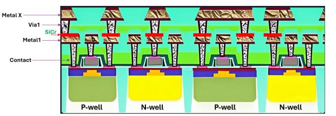
- Gate metals, plug/contact, barrier/seed layers, top metal
- RF electrode/IDT
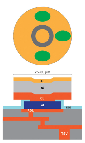
- Advanced packaging UBM, RDL
- 3D NAND Hard mask
- MEMS Poly/Ge
- Low-k, ultra low-k film modulus, implant, thermal conductivity

Enabling In-Line Process Control for Hybrid Bonding Applications
Using Picosecond Ultrasonic Technology for AI Packages, Part 2
Front-End Technologies Are The New Back-End Tools: Using Picosecond Ultrasonics Technology For AI Packages, Part 1
Picosecond Ultrasonics: An Advanced Technology Utilized for Process Control of SiCr Thin Film Resistors
Advanced Interconnect Process Control with Picosecond Ultrasonic Technology for AI Device Packaging
Applications of Picosecond Laser Acoustics for Advanced Packaging
Using Picosecond Ultrasonics To Measure Trench Structures In SiC Power Devices

The Road to SiC Process Control
Optimizing Metal Film Measurement on IGBT And MOSFET Power Devices with Picosecond Ultrasonic Technology
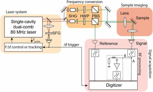
Efficient pump-probe sampling with a single-cavity dual-comb laser: Application in ultrafast photoacoustics
Paving the Way for 5G: RF Filter Process Monitoring and Control Using Picosecond Ultrasonic Metrology
Imaging of Overlay and Alignment Markers Under Opaque Layers Using Picosecond Laser Acoustic Measurements
Advantages of Picosecond Ultrasonic Technology for Advanced RF Metrology
Full Metrology Solutions for Advanced RF with Picosecond Ultrasonic Metrology
Monitoring Critical Process Steps in 3D NAND using Picosecond Ultrasonic Metrology with both Thickness and Sound Velocity Capabilities

Do you have an Echo system question? Let’s talk!
As your partner for innovative solutions, we’re always here for you.
Discover how our cutting-edge semiconductor solutions are engineered to meet your most complex challenges: delivering performance, reliability and innovation where it matters most.
Let’s Talk
"*" indicates required fields