

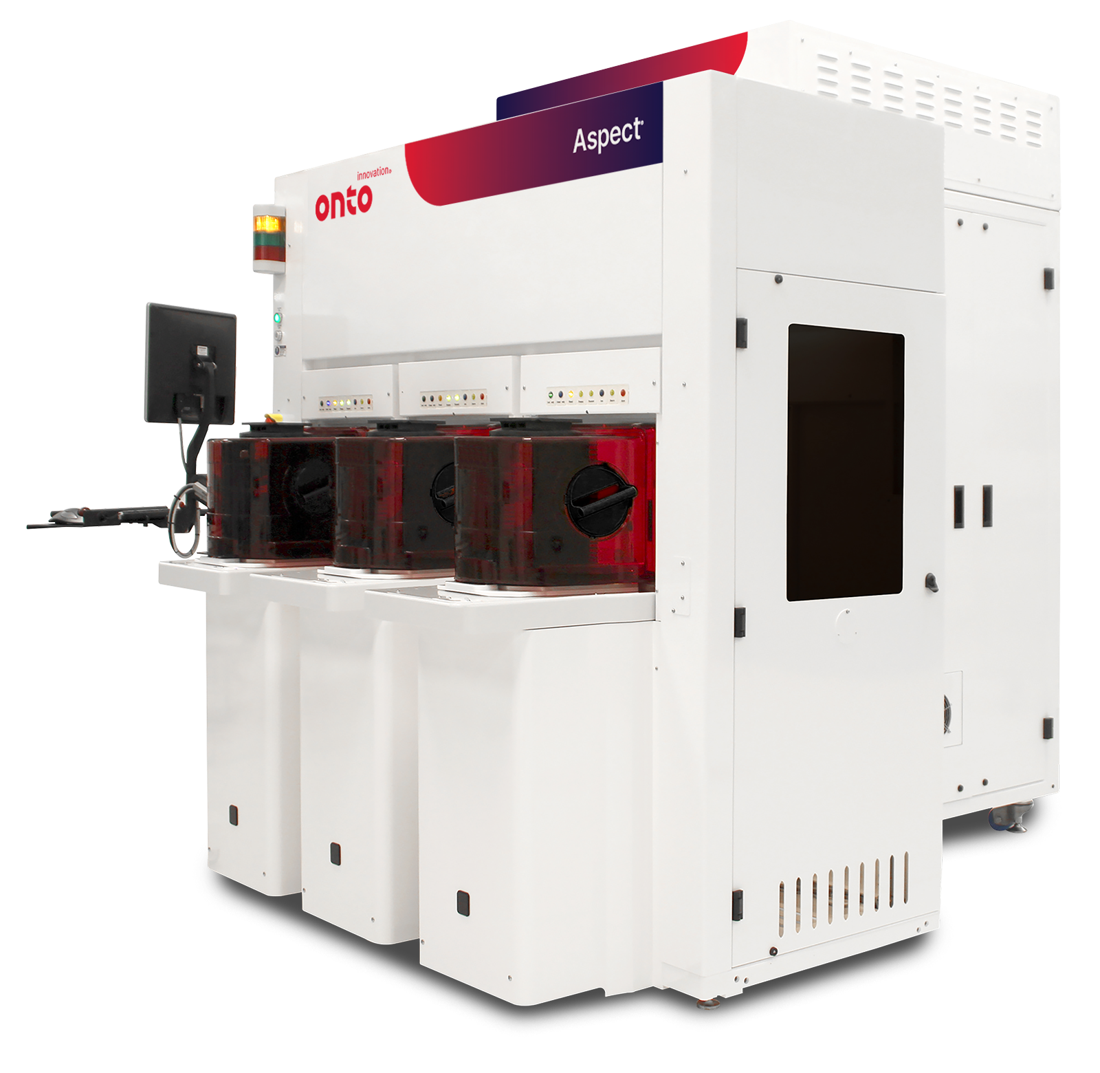
Aspect® System
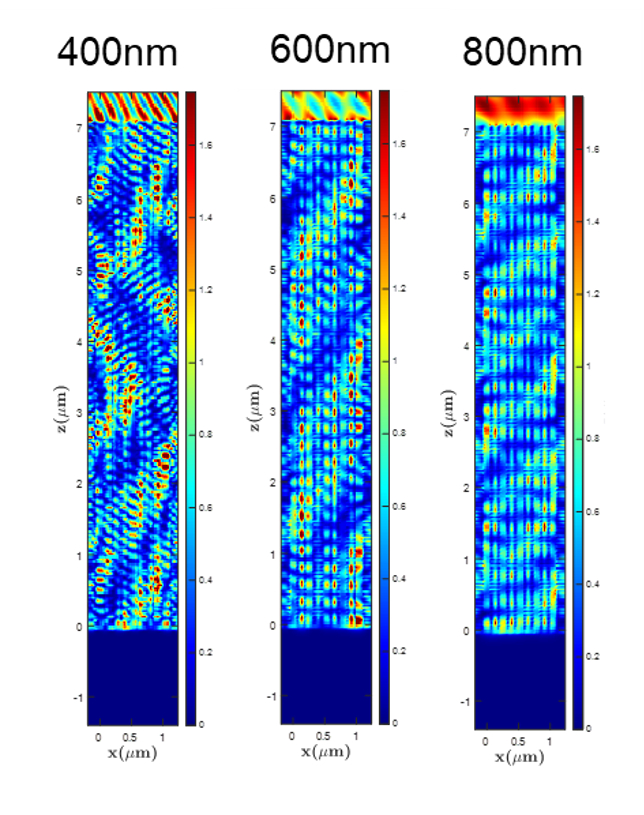
The Aspect System is a revolutionary in-line, non-destructive infrared optical critical dimension (IRCD) system measuring Z-dimension profiling of high aspect ratio structures to enable critical process control. It meets the needs of leading-edge customers with its high speed and process coverage.
Product Overview
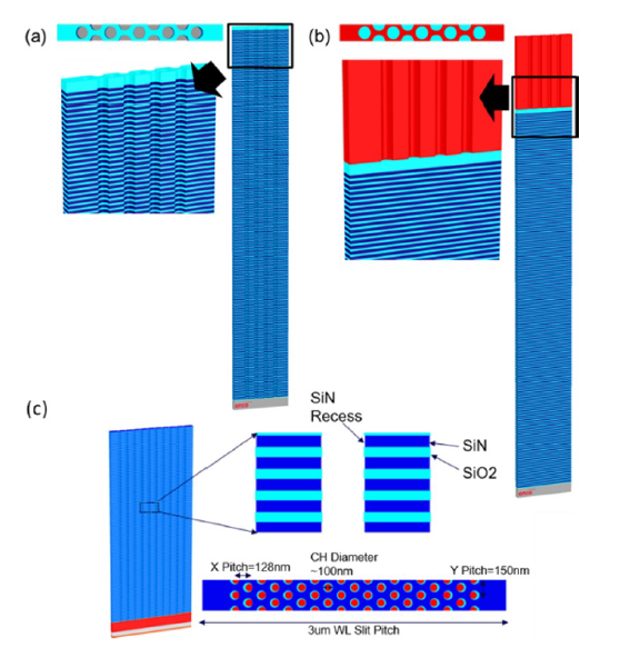
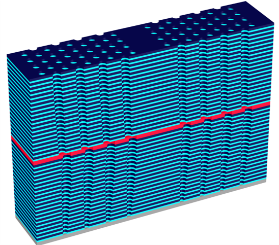
As the semiconductor industry relentlessly pursues density and power scaling, more and more high aspect ratio (HAR) processes are used across multiple device segments, especially in advanced memory such as 3D NAND and 3D DRAM. The Aspect metrology system was designed with these ongoing architectures and scaling strategies in mind. Aspect metrology has demonstrated superior performance across multiple customer devices through a unique proprietary IRCD system that provides full profiling capability to enable critical process control, with the speed and process coverage that customers require.
The Aspect system is powered by a software analysis engine, Ai Diffract™, that provides up to 90% faster time to solution which extends the industry leading NanoDiffract® software by leveraging extensive machine learning capabilities along with high fidelity modeling. The result is a simultaneous improvement in metrology performance along with a significant time to solution reduction.
Applications
- Etch, cleans, and deposition for 3D NAND
- Etch, cleans, and deposition for 2D and 3D DRAM
- Deep trench etch and doping for CIS
- Deep Trench etch in Power Devices
- On-device materials characterization for EPI process
Featured Markets
Hybrid Bonding Process Control Solution
Hybrid bonding enables ultra-dense 3D memory interconnects with up to 1,000x more connections than microbumps. Achieving high yield requires stringent process control, including monitoring topography and detecting particles, cracks and voids. Measuring dishing in copper pads provides valuable insight into surface conditions. Together, these process control insights contribute to improved device reliability and performance.

Enabling In-Line Process Control for Hybrid Bonding Applications
As demand grows for high-performance computing (HPC) and AI-driven applications, manufacturers are turning to hybrid bonding to enable the ultra-dense 3D integration required for next-generation chip architectures. This advanced packaging technology presents significant process challenges. Surface preparation must be precisely controlled to eliminate particles, excess recess, and copper pad dishing, all of which can compromise bond quality. During pre-annealing, particle-induced gaps and wide bonding gaps can prevent proper wafer contact. Post-annealing, the formation of dielectric and metal voids introduces further risks to electrical performance and long-term reliability.

Iris™ S System
The Iris S system is a versatile platform solution for the advanced packaging and specialty market, supporting 150mm, 200mm and 300mm wafers. It provides thin and thick film, OCD and wafer bow and film stress measurements.

IMPULSE® V System
The IMPULSE V system helps to advance CMP processing with enhanced wavefront technology and AI-driven analytics, delivering over 2X precision improvement and faster solutions, crucial for next-gen semiconductor manufacturing demands.

Dragonfly® G5 System
The Dragonfly G5 system is engineered for inline process control of leading-edge advanced packaging technologies. As the latest generation pattern inspection system in the Dragonfly series, it delivers unparalleled accuracy in detecting submicron defects and performing high-resolution 3D measurements.

Aspect® System
The Aspect System is a revolutionary in-line, non-destructive infrared optical critical dimension (IRCD) system measuring Z-dimension profiling of high aspect ratio structures to enable critical process control. It meets the needs of leading-edge customers with its high speed and process coverage.

Atlas® V System

Atlas® III+ System
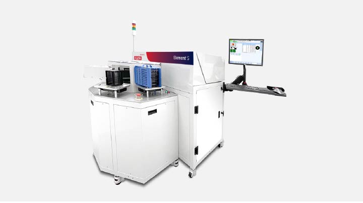
Element™ S System
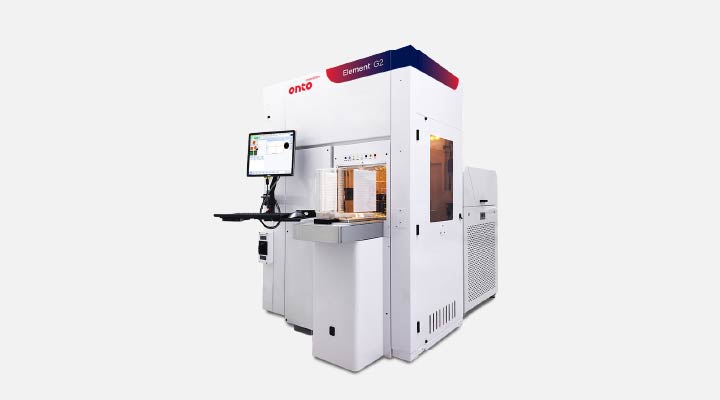
Element™ G2 System
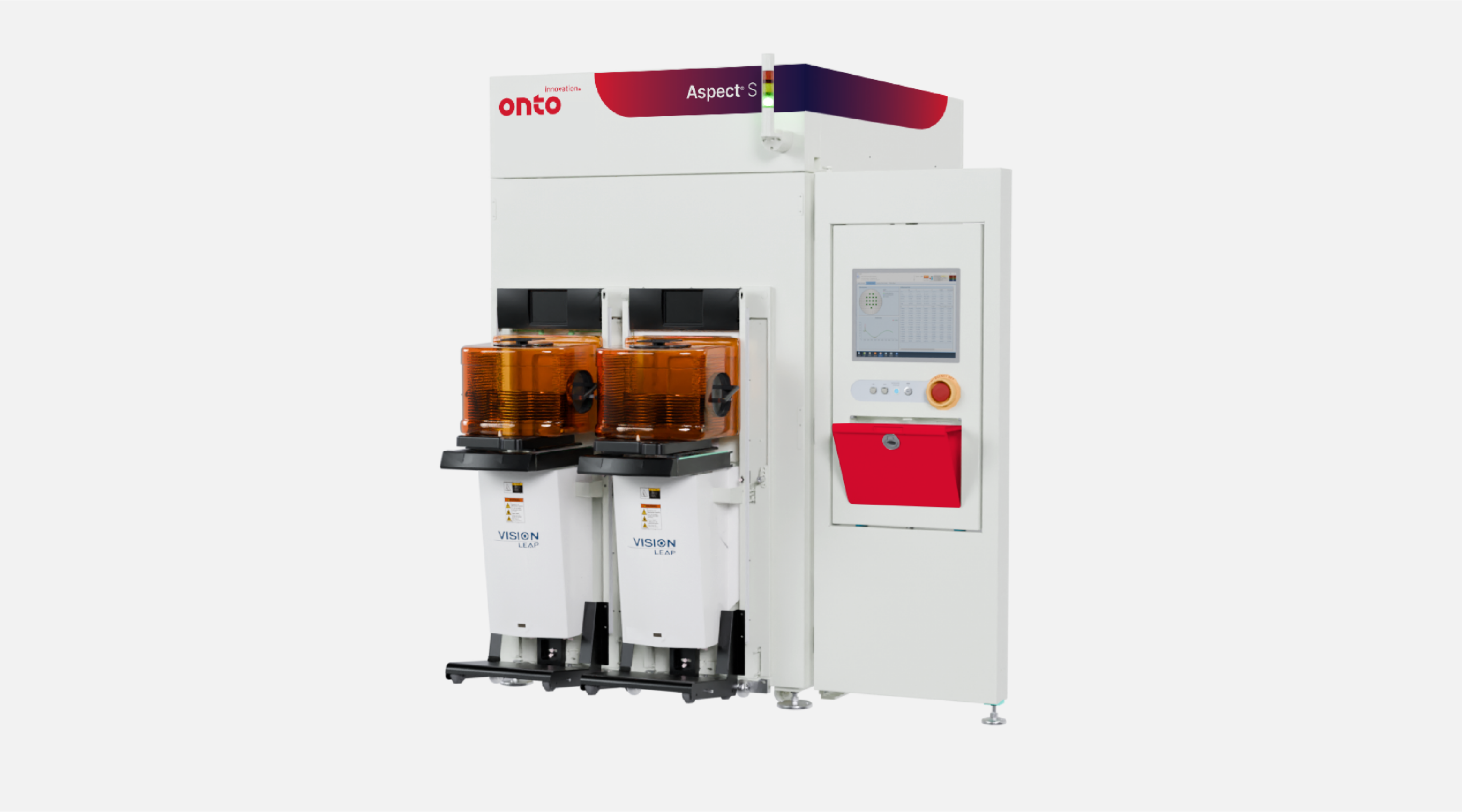
Aspect S System
Mid-infrared ellipsometry for optical critical dimension metrology
Non-destructive Measurement of Bottom Width in Deep Trench Isolation Structures Using IRCD Metrology
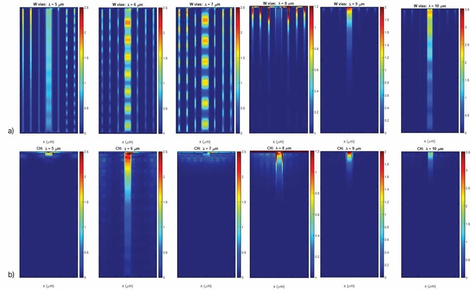
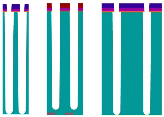
3D NAND Needs 3D Metrology
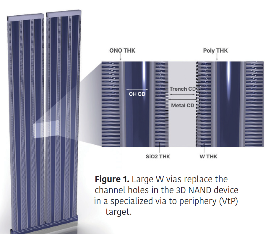
Measuring the Critical W-recess in 3D NAND
Critical Moves: Advanced Logic Devices And CIS Benefit From Applications Using IRCD Metrology
Mid-Infrared Optical Metrology for High Aspect Ratio Holes in 3D NAND Memory Manufacturing
Untangling 3D NAND: Tilt, Registration, and Misalignment

Do you have an Aspect system question? Let’s talk!
As your partner for innovative solutions, we’re always here for you.
Discover how our cutting-edge semiconductor solutions are engineered to meet your most complex challenges: delivering performance, reliability and innovation where it matters most.
Let’s Talk
"*" indicates required fields