

Overcoming Silicon Photonics Process Control Challenges in the AI Era
How connected inspection, metrology and software can help manufacturers move SiPh and CPO toward high-volume production
More bandwidth. Lower latency. Less power consumed and less heat generated.
These are three of the challenges facing manufacturers as AI pushes electrical interconnects toward their limits. Silicon photonics (SiPh) and co-packaged optics (CPO) offer a path forward by using light to transmit data rather than relying solely on electrical signals. But realizing those benefits at production scale introduces another challenge: maintaining precise process control across the optical structures, materials and integration processes that ultimately determine device performance and yield.
At the same time, traditional copper interconnects face increasing resistance, electromigration and power challenges as semiconductor architectures scale (Figure 1). For manufacturers, the shift toward silicon photonics places greater importance on precise control of optical structures and materials.
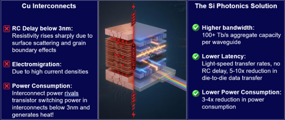
Figure 1: In the AI era, interconnects (within die and die-to-die and board-to-board) become the bottleneck.
One of the fundamental differences between conventional semiconductor manufacturing and silicon photonics is what manufacturers need to control.
Photonics yield and performance depend on critical dimensions and tight control of geometry, films and defects. Optical performance can be highly sensitive to relatively small process variations, with consequences for device performance and yield.
That makes several areas particularly important:
- Fiber connect (V-groove) geometry, which can affect fiber placement, alignment and coupling efficiency.
- Waveguide geometry and cladding, where height, width, sidewall roughness and taper, refractive index and cladding thickness influence light confinement and propagation, along with defects located on the waveguide facet itself.
- Microlenses, where defects, shape, placement and material nonuniformity can degrade transmission, beam shaping and coupling.
- Laser devices, which require control of geometry, films and defectivity.
- Die attach, die level bow/warp, micro bumping, through silicon vias (TSVs) and related integration structures, where geometry and defects can affect optical and electrical performance.
The result is a process control challenge that extends across multiple inspection and metrology steps. Manufacturers need visibility into the different variables that influence optical performance throughout fabrication and integration.
Process Control for Critical SiPh Structures
This is where the value of Onto Innovation’s SiPh process control portfolio becomes most apparent.
Rather than treating photonics as one measurement problem, Onto combines inspection, 2D and 3D metrology, optical critical dimension (OCD) and film metrology, overlay and dimensional metrology, and enterprise software across multiple SiPh manufacturing steps. The portfolio applies Onto’s semiconductor process control experience from bare silicon through advanced packaging to the specialized structures used in photonic devices.
Consider the V-groove used to position optical fibers relative to a photonic integrated circuit. V-groove geometry and particle defects present can directly affect fiber alignment and coupling efficiency. Onto’s portfolio supports inspection of defects as well as measurements of V-groove critical dimensions, depth and sidewall angle, alongside waveguide parameters including CD, thickness, refractive index and facet angle (Figure 2).
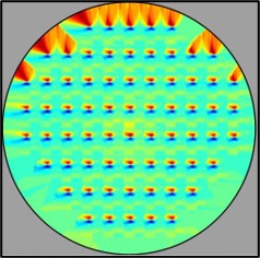
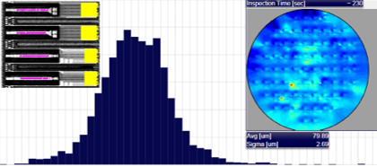
Figure 2: (Left) V-groove critical dimension, (right) V-groove depth metrology.
The portfolio supports high-speed 3D metrology with 100% wafer coverage for this application. Early detection of misprocessing can help manufacturers avoid downstream scrap and protect production efficiency.
Waveguides create another demanding control problem. Onto’s SiPh portfolio addresses measurements including dielectric cladding thickness; silicon, germanium, low-temperature oxide (LTO) or polymer thickness; refractive index; pattern alignment; CD; height; and sidewall and facet angles. Systems including Iris™, IVS® 380, Dragonfly® system and its 3Di™ Technology, Echo™ and Discover® software support different steps in these processes.
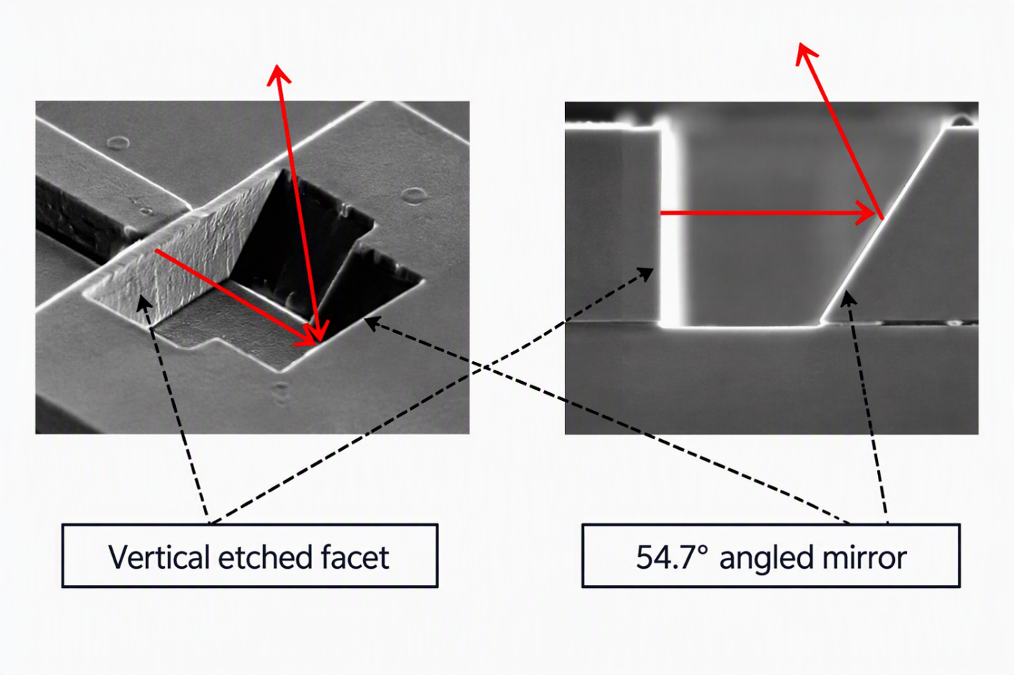
Figure 3: Facet measurement images supporting post-etch or post-saw angle metrology.
Facet control illustrates why this sensitivity matters (Figure 3). Onto has demonstrated sensitivity to a 0.06-degree change in facet angle, demonstrating the level of control required because facet geometry, roughness and films can influence optical coupling efficiency, reflection and fiber-alignment sensitivity.
Extending Process Control
The same process control approach extends to structures beyond waveguides and V-grooves.
For microlenses, Onto’s SiPh portfolio addresses inspection and metrology from incoming glass through lithography, reflow, shape-transfer etch, cleaning and post-dice inspection. Manufacturers can employ the PrimaScan™, IVS 380, Dragonfly platform and Iris systems, along with Discover software, in different stages of this process flow.
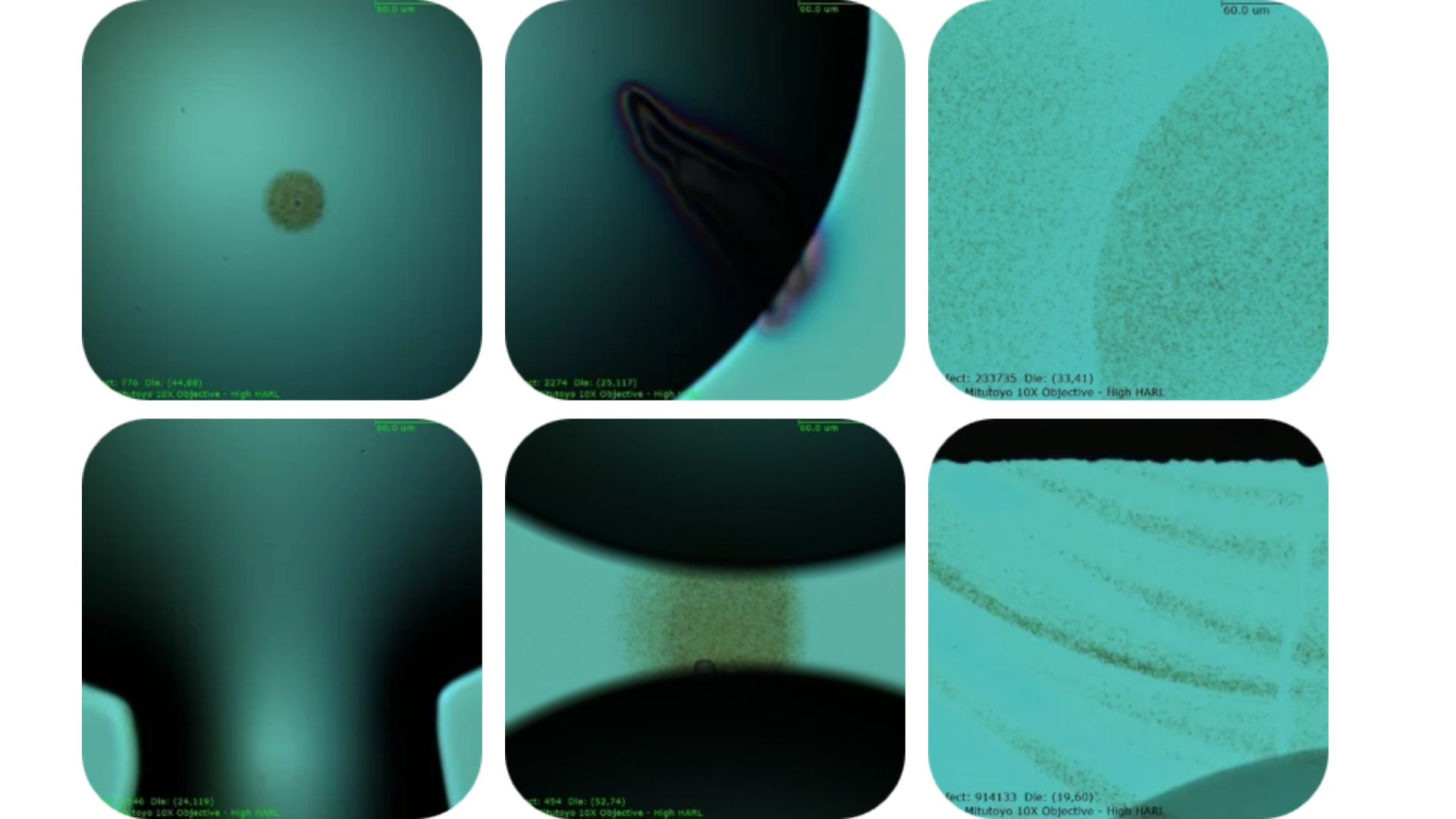
Microlens control matters because shape, placement, material nonuniformity and defects can translate into optical loss, channel imbalance and packaging yield loss in photonic integrated circuit (PIC) and CPO architectures (Figure 4).
Figure 4: Examples of microlens defects.
Onto’s portfolio also addresses laser-device process control. Inspection and metrology requirements include epitaxial layers, mesa geometry, contact metal thickness, final optical quality inspection and post-dice inspection. Onto addresses these requirements with a combination of inspection and metrology solutions, including Element™ G2, Aspect® S, Iris S, Echo and Dragonfly systems and Discover software.
This breadth of products is important because SiPh manufacturing encompasses a sequence of optical, dimensional, material and defect-control challenges. Addressing those interconnected challenges requires inspection, metrology and software across critical photonic structures and the advanced packaging processes required for CPO.
Connected Process Control
Inspection and metrology data are most valuable when manufacturers can turn those measurements into process insight. Onto combines inspection and metrology technologies with software and analytics to connect information across tools, modules and process steps. For SiPh manufacturers, that connected approach can support faster root-cause analysis, earlier identification of process excursions and learning as processes progress toward high-volume production.
In addition, Discover software supports defect, yield and run-to-run use cases across V-groove, waveguide, microlens and module-assembly applications, connecting inspection and metrology data across the manufacturing flow.
SiPh Meets Advanced Packaging
These process control challenges broaden further as silicon photonics is integrated into CPO architectures.
CPO manufacturing depends on considerably more than control of the photonic structures themselves. Hybrid bonding, interposers, TSVs, overlay, die placement, redistribution layers and bumps are among the heterogeneous integration challenges manufacturers must address.
Module assembly introduces additional requirements including wafer and die warpage, stack height and tilt, bump inspection, pre-hybrid-bond inspection, hybrid-bond pad recess measurement, optical via inspection and metrology, and post-dice inspection for particles and hidden microcracks. The Dragonfly, Iris S and Discover systems provide the inspection, metrology and process control capabilities manufacturers need to address these module assembly requirements.
Together, this portfolio provides manufacturers with a process control approach spanning the photonic device and its integration into increasingly complex CPO architectures. Onto’s coverage extends across wafer- and panel-level integration, with inspection, metrology and lithography touchpoints spanning SiPh and advanced packaging.
A Path Toward High-Volume Manufacturing
For manufacturers, scaling SiPh ultimately depends on maintaining control as photonic devices move through increasingly complex fabrication and integration processes. Small variations that begin at the structure or material level can carry consequences into optical performance, assembly and yield.
Onto Innovation’s SiPh suite brings inspection, metrology and software across V-grooves, waveguides, microlenses, laser devices, module assembly and advanced packaging, giving manufacturers greater visibility across the manufacturing flow.
As SiPh and CPO scale, connecting that process data can help manufacturers identify excursions earlier, accelerate learning and build the process control needed to move optical technologies confidently toward high-volume production.
Timothy Kryman is Senior Director of Product Marketing at Onto Innovation, where he leads strategic product positioning and market development for advanced semiconductor process control solutions.
You Have a Challenge? Let’s talk.
We’d love to connect with you.
Looking to learn more about our innovative solutions and capabilities? Our team of experts is ready to assist you. Reach out today and let’s starts a conversation about how we can help you achieve your goals.
Let’s Talk
"*" indicates required fields