A Clear Advantage: Precision Glass Carrier Inspection for AI and HPC Markets

If you’ve been following the evolution of advanced packaging, you know that the industry is pushing boundaries like never before. From high-performance computing to industry-upending AI devices, the demand for smaller, faster, and more powerful chips is driving innovation at every level. One of the unsung heroes in this transformation: Glass carriers.
These carriers are becoming essential for applications involving high-bandwidth memory (HBM), 2.5D/3D integration, and chiplet architectures. During the manufacturing process, glass carriers serve as mechanical support for thin wafers and panel-level packages. Why? Glass carriers are noted for their warpage resistance, superior rigidity, and thermal stability. This combination of glass’ exceptional flatness and rigidity enables the precise placement of dies and interposers. Additionally, glass is optically transparent, which allows through-glass alignment during bonding and stacking, a critical capability for 3D integration where multiple layers must be accurately registered.
The benefits of glass carriers, however, come with several challenges, none of which should come as a surprise to anyone who has ever handled glass, whether in the fab or at home. Glass is fragile and, as such, is prone to surface defects, subsurface inclusions, and residual stress. Each of these can negatively impact die attachment quality, interconnect reliability, and die yield.
Let’s take a look at three major yield-killing culprits.
Surface defects such as particles, pits, and scratches are among the most common issues and may occur during glass carrier handling and processing, compromising the structural integrity and performance of advanced packaging assemblies (Figure 1). Particles can interfere with the bonding process, leading to poor adhesion or electrical discontinuities, while pits and scratches can propagate stress points that weaken the carrier during thermal cycling or molding.
However, subsurface inclusions and organic contamination, which are often introduced during reclaim or cleaning, pose more critical challenges. Inclusions within the glass can create localized stress concentrations, while organic residues can reduce UV transmission and cause bonding failures. These contaminants are particularly problematic in high-density interconnect environments where optical clarity and surface purity are critical.

Figure 1: Common glass carrier defects
In addition to surface and subsurface defects, residual stress represents a concern. Over time, these stress points, manifesting during thermal processing or mechanical handling, can lead to cracks or delamination, undermining the thermo-mechanical integrity of the entire package.
These potential challenges are compounded each time a glass carrier is reused in an effort to reduce overall packaging costs. Fortunately, technologies have been developed to address this obstacle. These technologies integrate AI-driven defect classification, real-time analytics, and adaptive scanning modes to maintain throughput without sacrificing accuracy, enabling manufacturers to detect surface anomalies, subsurface inclusions, and stress-induced defects with unprecedented precision.
Enabling Defect-Free Glass Carriers
Today’s wafer-based inspection platforms utilize laser scatterometry and imaging techniques to inspect for nanometer sized defects on a variety of opaque and transparent/semi-transparent substrates. These substrates may be suitable for either R&D or high-volume advanced IC substrate (AICS) and fan-out panel level processing (FOPLP) environments. Proprietary inspection technology with multiple detection channels and advanced signal processing algorithms is applied to achieve accuracy and reliability in glass carrier inspection.

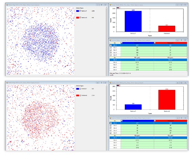
Figure 2: Results of top (blue) and bottom (red) defect mapping.
With each channel optimized to capture unique scattering and reflection signatures, the technology differentiates between surface and subsurface defects, as well as stress-related anomalies, with remarkable accuracy. Surface particles, scratches, pits, bumps, surface contamination, film or bulk wafer stress, voids/inclusions can be detected, measured, characterized, and imaged. One of the most significant capabilities of this technology is the ability to conduct simultaneous top, bottom, and internal defect mapping, a critical need for transparent and semi-transparent substrates where defects can occur across multiple planes (Figure 2).
Beyond defect detection, Angstrom-level film thickness measurement provides precise control over surface coatings and residual layers. This capability is particularly valuable in the glass reclaim process where even minor variations in film thickness can impact UV transmission and bonding performance. By enabling accurate defect detection and grading, only glass carriers meeting stringent quality standards are returned to production.
By introducing technologies that mitigate risks by providing comprehensive defect mapping and stress analysis, manufacturers are able to maintain the mechanical and thermal integrity required for next-generation devices. This capability is especially valuable in markets such as AI devices, high-performance computing, and automotive electronics where reliability is non-negotiable. With this combination of advanced optical technology and robust algorithmic analysis, manufacturers can successfully achieve higher yields, lower costs, and greater confidence in their packaging processes.
Conclusion
As packaging complexity grows and the use of glass carriers increases, inspection systems that combine multi-depth defect mapping and stress analysis will become indispensable for ensuring yield and reliability in AI and HPC devices. With the explosive growth in AI-driven data centers and advanced packaging architectures, manufacturers need solutions that combine accuracy, speed, and cost efficiency. The laser-based wafer inspection technology discussed in this blog meets several glass carrier challenges head-on while enabling advanced packaging houses to maintain defect-free glass carriers in support of next-generation advanced packaging.
The future of glass carriers is clear: with the right technologies at the ready, manufacturers have the tools and the means to meet the growing needs of the AI and HPC markets.
Biography
Jason Lin is Director of Product Marketing at Onto Innovation.

You Have a Challenge? Let’s talk.
We’d love to connect with you.
Looking to learn more about our innovative solutions and capabilities? Our team of experts is ready to assist you. Reach out today and let’s starts a conversation about how we can help you achieve your goals.
Let’s Talk
"*" indicates required fields
