

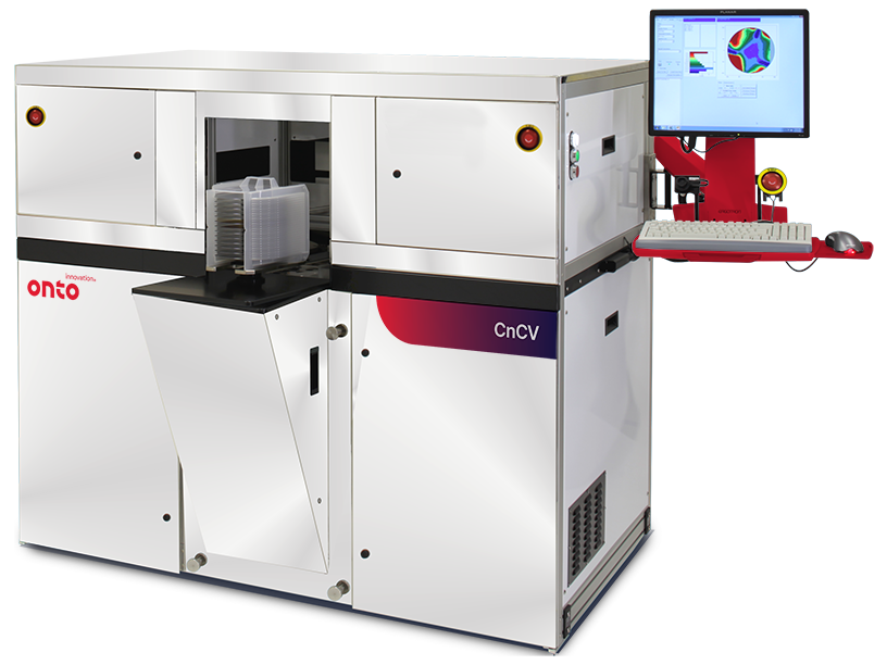
CnCV® System
The CnCV system enables wafer-level characterization of WBG materials without test device fabrication, reducing time and cost. As a mercury-free alternative to MCV, it eliminates contamination concerns. The enhanced Kinetic CV mode with UV-assisted corona charge neutralization achieves high throughput and precision for fast, reliable process control.
Product Overview
The CnCV system utilizes a novel constant surface potential corona charging, which enables the precision required over a large voltage range. The patented technology includes charge- and photo-assisted modes, especially suited for speed and precision on WBG materials and structures, including SiC, Ga2O3, GaN, and AlGaN/GaN HEMT. Additionally, Corona-Kelvin characterization includes electrical properties of dielectrics and interfaces of films on SiC and GaN epi layers. An automated top-side edge contact (TSEC) is also available enabling characterization of WBG on insulating/semi-insulating substrates. Automated bias-temperature stress (BTS) measurements are also available with the CnCV system, providing a fast, noncontact way to quantify the reliability of passivated SiC and GaN.
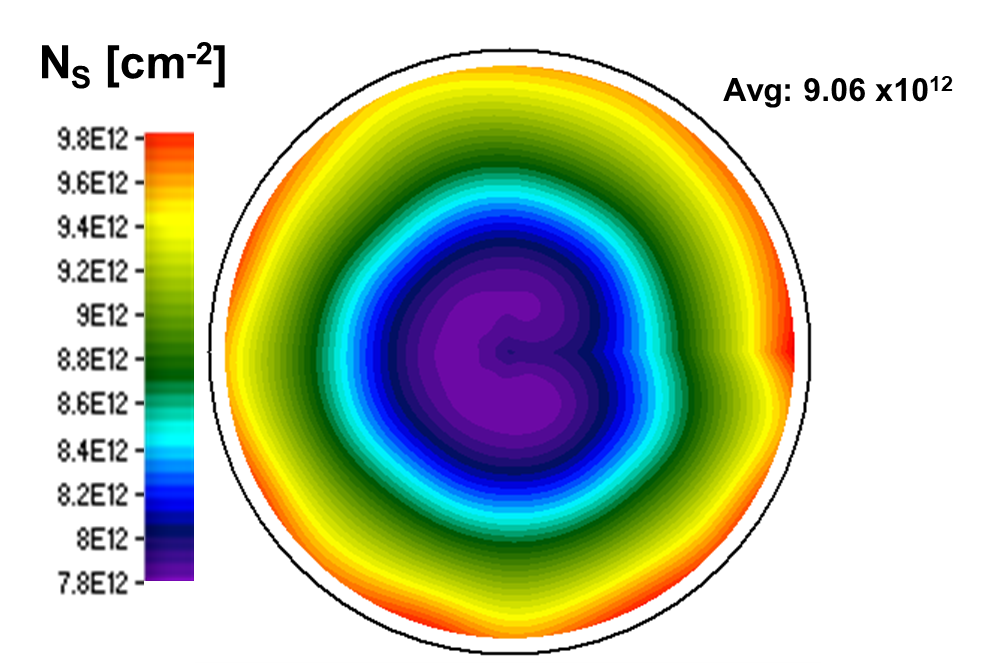
Beyond typical CV type parameters, the full wafer corona approach allows for QUAD (quality, uniformity, and defect) mapping. The electrical defect imaging, QUAD-EDI, mode is especially designed for SiC. It provides a unique means for quick screening of epi electrical defectivity enabling improvement in device yield prediction.

Figure 1. QUAD-EDI Map on final metallized device wafer after Merged Schottky PiN diode fabrication identifying failed dies.
Applications
- Non-contact epi dopant depth profiling in WBG materials
- AlGaN\GaN HEMT measurements (pinch off voltage & 2DEG sheet charge)
- Dielectric and interface characterization electrical defect imaging in SiC for yield prediction
- Bias-temperature stress (BTS) instability measurements on passivated WBG materials
Featured Markets
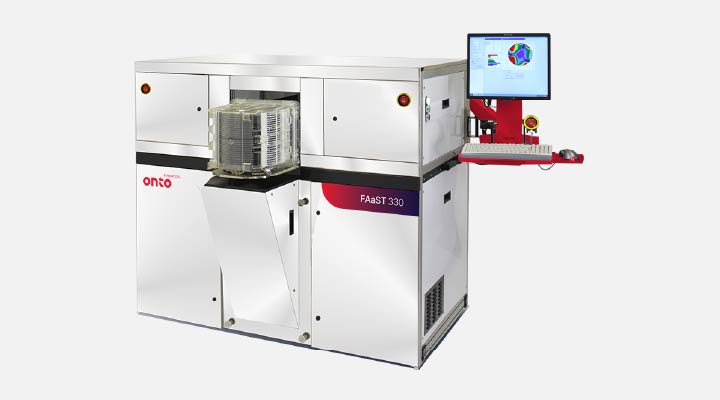
FAaST® Digital SPV System
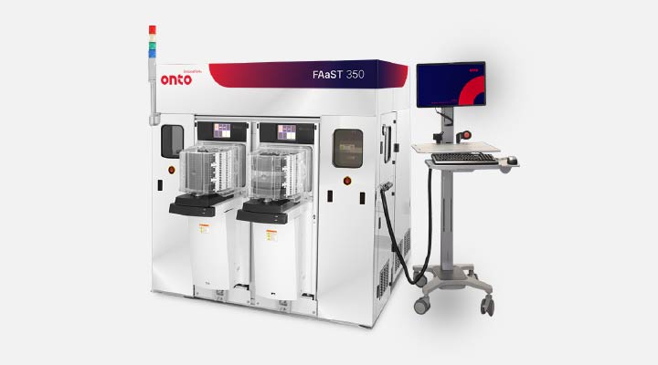
FAaST® CV/IV System
A Review of Recent Technological Advancements in Corona Noncontact Metrology Tools, CnCV, for Industrial WBG Wafer Testing and Electrical Defect Related Yield Prediction

Do you have a CnCV system question? Let’s talk!
As your partner for innovative solutions, we’re always here for you.
Discover how our cutting-edge semiconductor solutions are engineered to meet your most complex challenges: delivering performance, reliability and innovation where it matters most.
Let’s Talk
"*" indicates required fields