

Abstract
In this period of tight chip supply, semiconductor fabs aim to test only known good parts at back-end module testers to maximize tester outputs.
Traditionally, semiconductor fabs produce hundreds of wafers, which are verified using functional product test programs. Tested wafers are then sent to OSAT (Outsourced Semiconductor Assembly and Test) houses for packaging and final unit testing. Units that fail package level testing are discarded, resulting in lost time and money spent on dicing, packaging and testing.
Based on teardown articles for the iPhone A13 Pro Max, the A15 Bionic chip costs approximately USD$45. Factoring in the average selling price (ASP) of a 5nm node wafer, yielding 95%, the packaging assembly test cost is close to 30% of the total chip cost.
Sending only good wafers forward is crucial. With packaging assembly test costs making up to ~30% of the total chip cost, it is cost effective to send wafers that are known/predicted to pass final package testing to OSAT houses. This ensures low rejection rates at the final package test step, resulting in higher finished goods out.
If the confidence level is high, product sort and final test package level testing can be avoided, saving additional test time and test cost.
Using historical data of product testing at the fab level and package final test data, a model was built (using Onto Innovation Discover® Yield AI Platform) to represent the performance of product testing at the fab level with final test data as output. Historical data from the fab / OSAT houses was prepared, and the model was trained using a DNN algorithm.
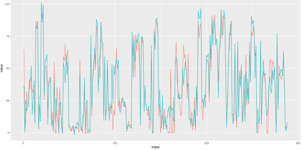
The final retrained model is deployed in a fab environment in a monitoring mode. Below shows actual vs predicted results overlaid using the ML DNN model.
The model deployed into production predicts the final test yield of wafers at the end of the line, allowing product engineering to monitor the line more efficiently. “Bad” wafers are automatically tagged in the MES system with an assigned wafer grade Last to Ship (LTS). Fab real time dispatching will dispatch and move wafers with the assigned wafer grade to a wafer bank labeled “Last to Ship.” Non LTS wafers are shipped automatically to OSATs, ensuring only good parts are sent to the back-end packaging house for dicing, packaging and ultimately integration into a MCM (Multi Chip Module).
Event Details
Event: AEC/APC Symposium Asia| Date | Nov 26, 2025 |
|---|---|
| Time | 10:50 a.m. - 11:10 a.m. JST |
| Location | Fukuoka, Japan |
| Event | AEC/APC Symposium Asia |
| Presenters |