

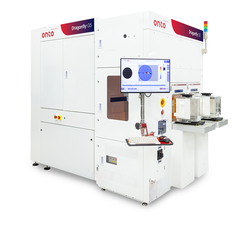
Dragonfly® G5 System
The Dragonfly G5 system is engineered for inline process control of leading-edge advanced packaging technologies. As the latest generation pattern inspection system in the Dragonfly series, it delivers unparalleled accuracy in detecting submicron defects and performing high-resolution 3D measurements.
Product Overview
Designed to meet the demands of advanced semiconductor technologies, the Dragonfly G5 system is purpose-built to deliver high-performance, reliable inspection and metrology across complex heterogeneous integration processes. Leveraging next generation high speed line scan 2D imaging and custom-engineered objectives, the system achieves over 3X throughput improvement compared to its predecessor, with submicron sensitivity down to 150nm.
Continuing the legacy of innovation, the Dragonfly G5 system introduces a multi-angle illumination channel that significantly improves signal-to-noise ratio for faint defect detection. Combined with powerful AI-driven algorithms, it enhances both the detectability and classification of critical, yield-impacting defects–empowering fabs to maintain quality and accelerate time-to-yield.
The Dragonfly G5 system expands process control flexibility for wafer-to-wafer and die-to-wafer bonding by integrating high-speed IR imaging to detect sub-surface defects. It incorporates the latest generation of 3Di™ technology, extending bump height metrology capabilities to support next-generation microbumps essential for 3D integration. This enables additional inspection and metrology touchpoints across increasingly complex packaging architectures.
Applications
- Hybrid Bonding
- Redistribution Layers (RDL): after develop, after etch
- BS/FS Pad CMP
- TSV Reveal
- Micro bumps and Cu pillars

Dragonfly® G3 System

EB40™ Module

Discover® Defect Software

Discover® Review Software

TrueADC® Software

Inspection Tool Productivity Software
Hybrid Bonding Process Control Solution
Hybrid bonding enables ultra-dense 3D memory interconnects with up to 1,000x more connections than microbumps. Achieving high yield requires stringent process control, including monitoring topography and detecting particles, cracks and voids. Measuring dishing in copper pads provides valuable insight into surface conditions. Together, these process control insights contribute to improved device reliability and performance.

Enabling In-Line Process Control for Hybrid Bonding Applications
As demand grows for high-performance computing (HPC) and AI-driven applications, manufacturers are turning to hybrid bonding to enable the ultra-dense 3D integration required for next-generation chip architectures. This advanced packaging technology presents significant process challenges. Surface preparation must be precisely controlled to eliminate particles, excess recess, and copper pad dishing, all of which can compromise bond quality. During pre-annealing, particle-induced gaps and wide bonding gaps can prevent proper wafer contact. Post-annealing, the formation of dielectric and metal voids introduces further risks to electrical performance and long-term reliability.

Iris™ S System
The Iris S system is a versatile platform solution for the advanced packaging and specialty market, supporting 150mm, 200mm and 300mm wafers. It provides thin and thick film, OCD and wafer bow and film stress measurements.

IMPULSE® V System
The IMPULSE V system helps to advance CMP processing with enhanced wavefront technology and AI-driven analytics, delivering over 2X precision improvement and faster solutions, crucial for next-gen semiconductor manufacturing demands.

Dragonfly® G5 System
The Dragonfly G5 system is engineered for inline process control of leading-edge advanced packaging technologies. As the latest generation pattern inspection system in the Dragonfly series, it delivers unparalleled accuracy in detecting submicron defects and performing high-resolution 3D measurements.

Aspect® System
The Aspect System is a revolutionary in-line, non-destructive infrared optical critical dimension (IRCD) system measuring Z-dimension profiling of high aspect ratio structures to enable critical process control. It meets the needs of leading-edge customers with its high speed and process coverage.

Do you have a Dragonfly G5 system question? Let’s talk!
As your partner for innovative solutions, we’re always here for you.
Discover how our cutting-edge semiconductor solutions are engineered to meet your most complex challenges: delivering performance, reliability and innovation where it matters most.
Let’s Talk
"*" indicates required fields