Abstract
As glass carriers gain traction in High Bandwidth Memory (HBM) advanced packaging architectures—particularly in 2.5D and 3D integration schemes—the demand for high-resolution, non-destructive inspection methodologies becomes increasingly critical. These carriers offer a rigid, flat, and thermally stable platform that significantly reduces warpage during high-temperature packaging processes such as reflow, bonding, and molding. However, despite their mechanical advantages, glass carriers are inherently susceptible to a variety of defect modes that can negatively impact both manufacturing yield and long-term device reliability. Common defect types include surface particles, pits, and scratches, as well as subsurface inclusions, organic contamination, and residual stress. These defects can degrade the thermo-mechanical integrity of the package and impair interconnect performance, posing serious challenges for high-density integration.
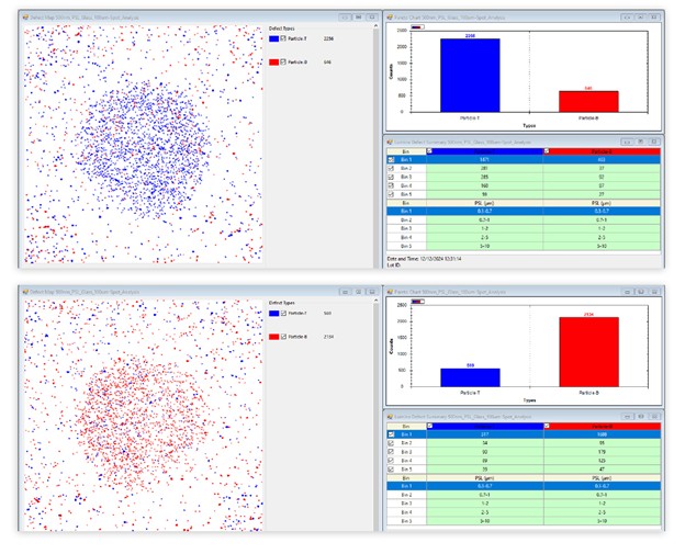
A laser-based line scanning system has been developed to address these challenges. This advanced inspection system integrates multi-channel optical detection with sophisticated processing algorithms to enable precise spatial classification of defects. The system not only identifies defects based on their unique scattering and reflection characteristics but also provides positional discrimination across the top, bottom, and internal planes of the glass substrate. A dedicated channel employs polarization signal analysis to detect organic/inorganic surface contamination and quantify the area/defect induced by residual stress, while also achieving Angstrom-level resolution in relative film thickness measurements. This capability is particularly vital for monitoring the glass reclaim process, where residual organics could reduce UV transmission and lead to bonding failures.
Beyond defect detection, the system offers comprehensive geometric analysis of the substrate, including warp and bow measurements, with a repeatability variation of less than 3%. These metrics are essential for ensuring precise die-to-carrier alignment and maintaining planarity in multi-die stacking configurations. The system’s architecture is designed to eliminate the need for mechanical chucks or spinning stages, thereby reducing the risk of mechanical damage during inspection—an important consideration when handling delicate and thin glass materials either panel or wafer shape.
This work presents the architecture, detection principles, and performance metrics of the laser-based line scanning system, emphasizing its role in process control, incoming material qualification and yield enhancement for the next generation of HBM advanced packaging technologies.
Event Details
Event: SEMICON West| Date | Oct 7 — Oct 9, 2025 |
|---|---|
| Time | 11:00 a.m. |
| Location | Phoenix, AZ |
| Presenters |
|


