Posted on Feb 2, 2024
The Great Lithography Debate: Copper Clad Laminate or Glass Substrates?
from Chip Scale Review
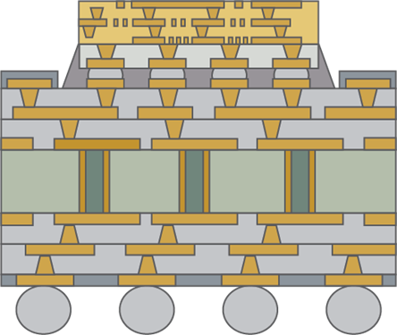
The number of defects detected through inspection is exploding at each new process node. There are now millions of defects being identified on each wafer, but only a fraction of those can cause problems.

Sept 2 — Sept 4, 2026
Onto Innovation is a proud exhibitor at SEMICON Taiwan.