
Measuring Multi-Layer Ultra-Thin Critical Films
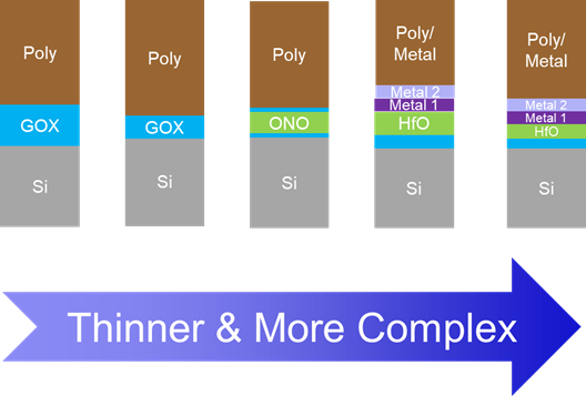
Artificial intelligence is one of the driving forces in today’s semiconductor industry, with more traditional market drivers like high performance compute and smart phones continuing to play important roles. This situation is unlikely change in the years ahead as chip makers continue their quest to create the most advanced nodes. With 3nm nodes in production and 2nm nodes on the horizon, the importance of film measurement only grows in significance as fabs seek to maintain the performance and reliability of cutting-edge devices.
Film metrology is an essential part of semiconductor manufacturing, whether you are dealing with material discovery, technology development, equipment or process control. In a typical semiconductor device manufacturing cycle, there are hundreds of film deposition and removal steps. In addition, film deposition and removal are also commonly used to monitor equipment health. Many of these steps use film measurement tools to ensure that equipment and processes are meeting production requirement.